Die Attach Film adhesives
Conductive and Insulating die attach films
- Home

- Products
- Die Attach Materials
- Die Attach Films
Die Attach Films
Henkel’s LOCTITE ABLESTIK conductive die attach film (CDAF) and non-conductive die attach films are leading the way in enabling customers to design products with controlled bondlines. Designers using Henkel’s die attach films are better able to control uniformity of bondline thickness and eliminate die attach fillets commonly found when using paste adhesives.
LOCTITE ABLESTIK conductive die attach films (CDAF) allow lead frame package manufacturers the same process advantages offered by non-conductive die attach film processes: controlled fillets, controlled bondlines, elimination of die tilt and better design latitude with the elimination of the die attach fillet.
Non-conductive die attach films combine dicing die attach tapes and film into a single product: dicing die attach film (DDF). Henkel’s DDFs enable packaging specialists using thinned die processes the added design latitude of designing processes with improved wafer stability, controlled bondlines, elimination of die tilt and the ability to do away with the dispensing processes.
Henkel's Conductive Die Attach Film (CDAF) Solutions Henkel was the first to develop and introduce conductive die attach film (CDAF) to the semiconductor market. A groundbreaking market development, this innovation was viewed by the semiconductor industry as a significant enabling technology to produce more capable and cost-effective leadframe package designs. Indeed, this has been the result, as numerous semiconductor packaging specialists have leveraged Henkel’s CDAF advantages for new and better package designs.
LOCTITE ABLESTIK CDF100 was the premier material in Henkel’s CDAF line and, since then, we have also developed second-generation pre-cut and dicing tape materials that have expanded the suite of conductive films to address various leadframe and laminate package requirements. Each material offers different properties and characteristics – from dicing die attach capability to varying thermal and electrical performance to cost competitiveness – but all of them deliver the undeniable advantages of film-based materials over that of conventional die attach paste.


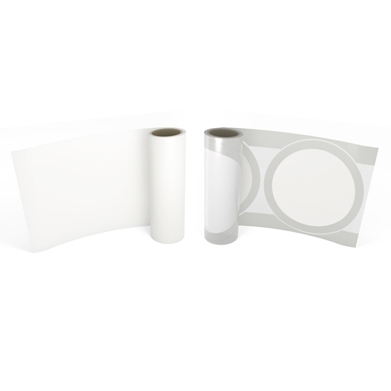
LOCTITE ABLESTIK ATB F150E
- 50um
- Non Conductive
- Wafer lamination and Chip on chip
- No longer available


Product Selector Guide
| Product | Description | Film thickness (um) | Moisture sensitivity level, MSL | Volume resistivity (ohm-cm) | CTE a1 | CTE a2 | Glass transition temperature (Tg) | Thermal conductivity (W/m-k) | In-package thermal resistance (K/W) | Key attributes |
|---|---|---|---|---|---|---|---|---|---|---|
| Loctite Ablestik CDF 200P | Ag-filled die attach adhesive | 15 or 30 | L1 260°C capable | 0.0014 | 50 | 120 | 15 | 2.3 | 1.5 | - Suitable for small die - Recommended for thin wafer handling applications - Oven cure |
| Loctite Ablestik CDF 300P | Ag-filled die attach adhesive | 15 or 30 | L1 260°C capable | 0.0010 | 50 | 200 | 10 | 1.0 | 2.1 | - Suitable for small die - High adhesion - Good wetting - Oven cure |
| Loctite Ablestik CDF 500P | Ag-filled die attach adhesive | 15 or 30 | L1 260°C capable | 0.0002 | 60 | 240 | 10 | 1.5 | 1.4 | - Good wetting and low warpage for large die - Recommended for thin wafer handling applications - Oven cure |
| Loctite Ablestik CDF 625P | Ag-filled die attach adhesive | 25 | L2 260°C capable | 0.0008 | 75 | 320 | -5 | 1.0 | 2.1 | - Low stress and excellent wetting for large die - Compatible with various metal surfaces, including solder - Oven cure |
| Loctite Ablestik CDF 700P | Ag-filled die attach adhesive | 15 or 30 | L1 260°C capable | 0.0002 | 35 | 160 | 30 | 5.5 | 0.7 | - Suitable for small and medium die - High adhesion - Oven cure |
| Loctite Ablestik CDF 815P | Ag-filled die attach adhesive | 15 | L1 260°C capable | 0.0003 | 40 | 120 | 10 | 3.4 | 0.7 | - Suitable for small die - Recommended for thin wafer handling applications - Oven cure |
| Product | Description | Dicing tape | Film thickness (um) | Wafer thickness (um) | Moisture sensitivity level, MSL | Modulus at 25°C (MPa) | Key attributes |
|---|---|---|---|---|---|---|---|
| Loctite Ablestik ATB 100 | Silica-filled, rubberized epoxy die attach adhesive | Non-UV | 25 or 30 | Up to 75 | L2 260°C capable | 1,170 | - Compatible with Cu wire or Au wire packages - Excellent wetting - Compatible with stealth dicing before grind (SDBG) process - Oven cure |
| Loctite Ablestik ATB 100HA | Silica-filled, epoxy die attach adhesive | UV/Non-UV | 20, 25 | Up to 50 | L1 260°C capable | 2,299 | - Consistent dicing and die pickup for large die applications - No passivation damage - Compatible with stealth dicing before grind (SDBG) process - SkipCure |
| Loctite Ablestik ATB 110U | Silica-filled, rubberized epoxy die attach adhesive | Non-UV | 10, 20, 30 | Up to 75 | L2 260°C capable | 875 | - Compatible with Cu wire or Au wire packages - No passivation damage - Compatible with stealth dicing before grind (SDBG) process - Fast oven cure |
| Loctite Ablestik ATB 120U | Silica-filled, rubberized epoxy die attach adhesive | Non-UV | 85 | - | L2 260°C capable | 875 | - Excellent gap filling ability - Non conductive - Thin bondline |
| Loctite Ablestik ATB 100US | Silica-filled, epoxy die attach adhesive | UV/Non-UV | 5, 10, 15, 20, 25 or 30 | Up to 50 | L2 260°C capable | 1,277 | - Consistent dicing and die pickup for large die applications - No passivation damage - Long thermal budget (4 hr. at 175°C) - Oven cure |
| Loctite Ablestik ATB F100E | Silica-filled, epoxy die attach adhesive | UV/Non-UV | 25 FoW: 35-80 FoD: 90- 150 | Up to 75 | L1 260°C capable | 5,256 | - Suitable for small to large die - Excellent workability for below 3mmX3mm die - Long work life (4 months before and after lamination) - Film over wire (FoW) and film over die (FoD) applications |
| Loctite Ablestik ATB F125E | Silica-filled, epoxy die attach adhesive | UV/Non-UV | 25 | 100 | L1 260°C at 2x2mm | 5,256 | - Ideal modulus for wide range of package sizes - Excellent workability for below 3mmX3mm die - Long work life (4 months before and after lamination) - Consistent dicing and die pickup for small die applications |
| Loctite Ablestik ATB F150E | Silica-filled, epoxy die attach adhesive | UV/Non-UV | 50 | 100 | L1 260°C at 2x2mm | 5,256 | - Ideal modulus for wide range of package sizes - Excellent workability for below 3mmX3mm die - Long work life (4 months before and after lamination) - Consistent dicing and die pickup for small die applications |
Frequently Asked Questions
Composition of conductive Die attach films
Looking at their core ingredients, conductive die attach films are fundamentally similar to paste versions. They are made from organic resin that may be thermoplastic or thermosetting, incorporated with a conductive filler, and dried into sheets/film of thickness ranging anywhere between 10-40 µm.
Polymer resins like epoxies, maleimides, bismaleimides, acrylates, silicone, cyanate esters have been used successfully in commercial films. And conductive fillers like gold, copper, silver, and nickel widely used.
Conductive die attach films are used as adhesives for circuit substrates, and heat sinks joined to metal or ceramic packages and PWBs. Silver-filled films are popular because of their high thermal conductivity in the order of 6 W/m·K. The typical electrical conductivities that make a film useful for EMI shielding lie in the range 5 × 10⁻³ to 5 × 10⁻⁴ ohm-cm.
Composition of Non conductive die attach films
Non-conductive die attach films are made from either thermoplastic or thermosetting polymer resin that is incorporated with a non-conductive filler. The composite is coated on a liner, and laminated on a carrier (for support) using pressure and heat.
Organic resins like epoxies, polyimides, bismaleimides, acrylates, silicone, cyanate esters and non-conductive fillers like silica, alumina, aluminum hydroxide, mica, glass, and organic fillers like PET have been used in manufacturing NCF.These films are electrically insulating to ensure the electrical integrity of circuits. They are used for maintaining the physical connection between the electrode pads and bumps in chip on board (COB) and chip on glass (COG) applications, and for safeguarding fine pitch devices.
Their thermal conductivity (1.5–1.6 W/m·K) comes into play for bonding heat-dissipating components to heat sinks.Manufacturers have also combined NCF and dicing tape into a single product to automate wafer processing and assembling
How should I preheat die attach films?
Most major conductive die attach film users are using chuck/substrate heating.
Heated collets on die bonders can also be used but they would require much tighter process control.
Using heated collets means running the risk to heat the Chip/CDAF in an uncontrolled way and make the wet-out become variable. The solution would be to run the die attach very slowly, to allow the temperature to stabilise, but that will give a low production output.
How do we handle large die PnP?
For large die, we recommend to have a “flat-face” pickup tool or collet with almost the same size as the die and multiple small vacuum holes (instead of a big hole in center). A rubber face with multiple small vacuum holes can minimise the loss of bonding force where the holes are located.
Finally, select a type of rubber that will withstand ~120C as the tool will get warm if used continuously.
Learn More
What is the typical structure of a Die attach Film?
A die attach film consists of a resin/hardener mix. Silver particles are dispersed into the resin/hardener mix, and these silver particles will form a conductive matrix after the film is cured with heat.
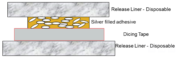
The adhesive film is normally supplied with protective layers of release liner on top & bottom. These can easily be removed and discarded. There is also a layer of dicing tape, which is used to support the wafer/adhesive film during the dicing process. The film can be laminated onto a wafer or onto a substrate at around 100°C. After this, it has sufficient adhesion for handling & processing the parts. And parts could be dis-assembled at this point, with heat or solvent. But we are not sure about electrical conductivity at this stage. High adhesion & good electrical conductivity is developed during a final heat cure at around 175C or 200C. After this final cure, it is near impossible to dis-assemble the parts.
Conductive Die attach films
Conventional die attach pastes are still plagued by inconsistencies that lead to voids, bleeds and uneven bondlines in assembled packages. This unreliability is an issue because the demand for smaller-sized semiconductor packages with increased functionality, like those used in many handheld electronics, keeps growing. Small-sized packaging calls for reduced footprint on a printed circuit board. This is accomplished by assembling multiple dies in the same package. When die attach pastes are used for die stacks, especially with difficult die-to-pad ratios, the challenges mentioned above can result in low yields.
Die attach films were created to solve the inconsistency issue in multichip modules and other applications involving wafer-level and die size limitations (e.g., thin dies ~100µm). In general, any situation where the problem of too little, or too much die paste can give rise to resin spreading (contaminating the die), large fillet formation (problematic for close die configurations), and resin overflow (causing poor wire bonding), films are the preferred solution.
Composition of conductive die attach film, DAF
Looking at their core ingredients, conductive die attach films are fundamentally similar to paste versions. They are made from organic resin that may be thermoplastic or thermosetting, incorporated with a conductive filler, and dried into sheets/film of thickness ranging anywhere between 10-40 µm. Polymer resins like epoxies, maleimides, bismaleimides, acrylates, silicone, cyanate esters have been used successfully in commercial films. And conductive fillers like gold, copper, silver, and nickel widely used.
Conductive die attach films are used as adhesives for circuit substrates, and heat sinks joined to metal or ceramic packages and PWBs. Silver-filled films are popular because of their high thermal conductivity in the order of 6 W/m·K. The typical electrical conductivities that make a film useful for EMI shielding lie in the range 5 × 10⁻³ to 5 × 10⁻⁴ ohm-cm.
Preparation of DAF
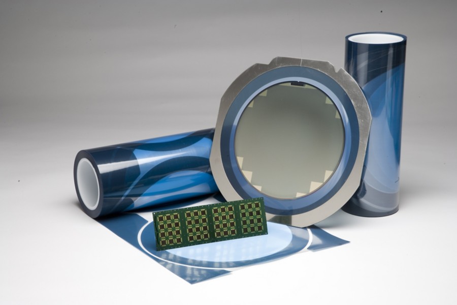
In general, a pre-mixed composite similar to die attach paste is coated onto a release liner, and together they are laminated to a reinforcement/carrier such as PVC or glass fabric. This provides structural support during fabrication and handling. Alternatively, for wafer-level applications, the resin composite plus carrier are laminated with dicing tape to produce dicing die attach film. It streamlines manufacturing and makes automation feasible, where cut wafer pieces are easily picked and positioned.
Film makers ensure the DAF and dicing tape have good bonding, and at the same time, the tape can be released without leaving residue on the film. UV and thermal release films are popular for this reason. Conductive die attach film can be purchased as:
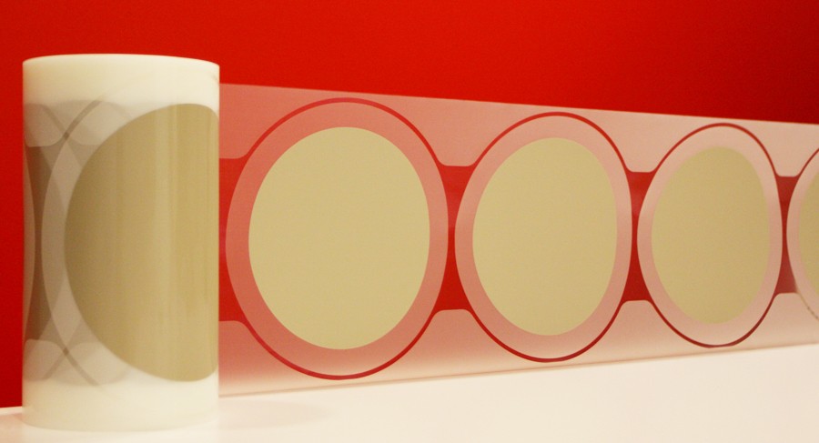
- Sheets or rolled sheets (e.g., 500 sheets per roll) that the user will cut into the desired shape to fit the die.
- Pre-cut sheets, sized for specific devices.
- Pre-attached to leadframes and substrates for extra convenience.
Properties that can affect conductive die attach film selection
Die mounting temperature
Supplier recommendations for bonding temperatures are a good place to start. The stipulated temperatures show the strongest bonding strength for specified materials. However, because the surfaces to be bonded can vary (roughness, type of material and level of contamination), the die attach process will need to be tested for each new product before scaling production.
Therefore, optimization is necessary to determine the bonding force, temperature, and bonding time that will achieve the strongest bond possible with minimum bondline thickness and negligible voids.
Tg, viscosity, and low stress
The stress characteristics of packages with film adhesives are a function of CTE, elastic modulus, and Tg to varying degrees.
Low modulus DAF can absorb a large amount of stress before fracture occurs. However, because the modulus for thin films at high temperatures is difficult to determine, adhesion at high temperatures is an important parameter when selecting a DAF variant. A DAF with high Tg is recommended at high temperatures. The Tg is the point (range) where the film changes from glassy solid to rubbery. As such, operating close to Tg means that the reliability of an assembly can become compromised. Testing the elastic modulus of a DAF at different temperatures is important.
Dicing
Optimizing the dicing parameters ensures dicing occurs with minimal chipping, cracking, or flying die. Die fly when the adhesion between DAF and dicing tape isn't strong enough. On the other hand, too strong an adhesion will lead to difficulties for die pick up. Appropriate film selection makes a trade-off between these competing challenges.
Good wetting
For handling thin wafers and large die sizes, films characterized with excellent wetting are recommended to enable complete and robust adhesion to substrates. This removes the need to apply excessive pressure that may damage the wafer. On the other hand, poor adhesion in large die can lead to warping and other problems.
Compatibility
For wafers, a film that is compatible with the various wafer processing stages will add a higher level of flexibility and performance to the manufacturing process. For other applications, the type of resin a film is composed of should agree with the substrate, whether metal, glass, ceramics or organics and also the end-use device. The manufacturer's guidelines will prove useful here.
Curing
With every application of heat, the film gets partly cured. This is not a significant issue for processes with few heating steps. However, for multichip packages, the total heat applied for heat treatment at wafer lamination, die attach and wire bonding needs to take into account the curing required for molding. There's a risk of delamination when attempting to mold packaging with fully cured DAF.
Certain films need heat and pressure to be applied simultaneously during curing, e.g., anisotropic films (so that metal filler particles become aligned) or where plastic substrates are involved (so that trapped air and volatiles can be pushed out). Techniques for preventing trapped air or moisture bubbles include curing under vacuum and vacuum baking surfaces before adhesion.
Storage:
DAF contains UV-sensitive components. Therefore, exposure to ambient light for periods of time can initiate curing. Rolled film can be stored from 6 months to a year (depending on the manufacturer) in a dark place before it loses its effectiveness.
Ideally, based on their storage time and minimum order quantity, DAF is suited to large scale manufacturing where these requirements will be matched by production volume to prevent wastage.
Non-conductive die attach films
The first die attach films to be manufactured were non-conductive. Moreover, their prices are not as prohibitive as conductive variants. Non-conductive films are useful for many of the same reasons: for preventing adhesive bleeding, voiding, and inconsistencies with bond line thickness.
They are required wherever multiple bare chips are to be stacked on top of one another since smaller package sizes help improve signal integrity and thermal path in modern packaging technology. Examples are 2.5D and 3D-TSV system in package (SIP) applications for high-end memory storage.
Advantages of non-conductive die attach films
The importance of no fillet in thin, small die and multiple die packaging
In traditional die attach paste applications, the leadframe pad is larger than the die. The applied paste flows and forms a fillet around the die edge but must not spread past and flow to the top surface of the die.
Die attach films make the dispensing step obsolete. In most cases, thermal compression bonding melts the film between a die and its substrate. As a result of negligible fillet formation or bleeding, die attach films are suitable for configurations demanding tighter clearance between die and die pad, making it possible to incorporate more die per package, such as in LGA and PBGA. In comparison, using pastes, larger die pad sizes means fewer dies per package are possible.
Processing and manufacturing are easier to control
A wafer already backed by die attach film eliminates the need to apply paste to individual die, essentially removing a repetitive stage from the manufacturing process. Also, no second guessing the thickness of the applied adhesive is required. The film thickness decides the width of bondlines.
The drawbacks of film are their higher price, the need for additional equipment, and generally, their lower thermal and electrical conductivity compared to paste variants. However, manufacturers are still coming up with films having higher thermal conductivities than their previous film products.
Die sizes:
Initially developed for devices using die sizes less than 3x3mm, film manufacturers continue to push the boundaries so their products are suitable for a wider range of die sizes. You will find that often, suppliers offer different grades of dicing die attach film depending on the size of the die. For smaller die sizes (2x2mm), increased adhesion to the dicing tape is implemented to prevent die flying off during dicing. Die attach films for sizes less than 1x1mm and thickness less than 100 µm are now available commercially.
Composition of non-conductive die attach film, NCF
Non-conductive die attach films are made from either thermoplastic or thermosetting polymer resin that is incorporated with a non-conductive filler. The composite is coated on a liner, and laminated on a carrier (for support) using pressure and heat. Organic resins like epoxies, polyimides, bismaleimides, acrylates, silicone, cyanate esters and non-conductive fillers like silica, alumina, aluminum hydroxide, mica, glass, and organic fillers like PET have been used in manufacturing NCF.
These films are electrically insulating to ensure the electrical integrity of circuits. They are used for maintaining the physical connection between the electrode pads and bumps in chip on board (COB) and chip on glass (COG) applications, and for safeguarding fine pitch devices. Their thermal conductivity (1.5–1.6 W/m·K) comes into play for bonding heat-dissipating components to heat sinks. As such, diodes, transistors, resistors, and thermal-sensitive integrated circuits can be mounted reliably to PCBs. Manufacturers have also combined NCF and dicing tape into a single product for adding flexibility to automated wafer processing and assembling.
Properties that can affect non-conductive die attach film selection
Dielectric strength and dissipation factor
To provide the required electrical insulation, a NCF will be characterized by low dielectric constant and low dissipation factor. Dielectric strength measures the likelihood of the film breaking down when exposed to a high enough voltage and becoming conductive as a result. Suppliers will state the maximum voltage a component featuring their NCF film can experience and still continue to operate normally.
A low dissipation factor indicates low power losses and the corresponding low heating of circuit components in close proximity.
Curing
Cure temperatures provided in supplier data sheets should achieve complete polymerization of the NCF and the strongest adhesive strength. At temperatures other than what is provided, poor wetting and severe reliability issues can result. Temperatures between 125-150°C for 1-2 s are common, although there are specialized formulations with lower cure temperatures and faster cure times which are attractive for multichip modules.
Voiding, and CTE
Even though compared to paste variants, films exhibit low voiding, voids can become an issue when films are not applied properly (100% void-free is unlikely, 5% is acceptable in many applications). A few factors that can contribute to voiding are the NCF's viscosity, thermal stability, chemical stability, the evenness of the adhering surfaces, and moisture absorption especially for plastic substrates (plastics have uneven surfaces and are hydrophilic). To overcome voids, users will need to address these factors, e.g., through pressure application, substrate preparation, filler selection, and so forth
The mismatch of the CTE of different packaging materials is often the direct cause of warpage that leads to cracking. Used as an adhesive, the selected NCF should be lower than the CTE values of the die and substrate to minimize mechanical stresses after bonding. The presence of voids combined with thermal expansion can lead to film failure.
Good wetting
For handling thin wafers and large die sizes, films characterized with excellent wetting are recommended to enable complete and robust adhesion to substrates. This removes the need to apply excessive pressure that may damage the wafer. On the other hand, poor adhesion in large die can lead to warping and other problems.
Storage
After UV exposure, some film variants deteriorate to such a level that the die pick up and place process is compromised. And due to their expense, it’s important to take into account the work-life of stored NCF.
Suitability to processing, and compatibility to various substrates
Wafers laminated with NCF will still need to undergo further processing conditions without degrading in adhesive and mechanical strength, or thermal properties, e.g., stealth dicing before grind (SDBG) process. Also, the selected film should exhibit excellent wetting and compatibility with typical substrates and applications, e.g., Cu and Au wire packages, solder masks, etc.
Applications for Die Attach Films
Conductive and Non Conductive Die attach Films can be used in a variety of packages and applications such as:
- Board on chip
- Leadframe semiconductor packages: QFN, QFP, SOIC, TSOP, and TSSOP
- Wirebond laminate packaging: Memory, RF sensors, Logic IC, MEMS and MOSFET