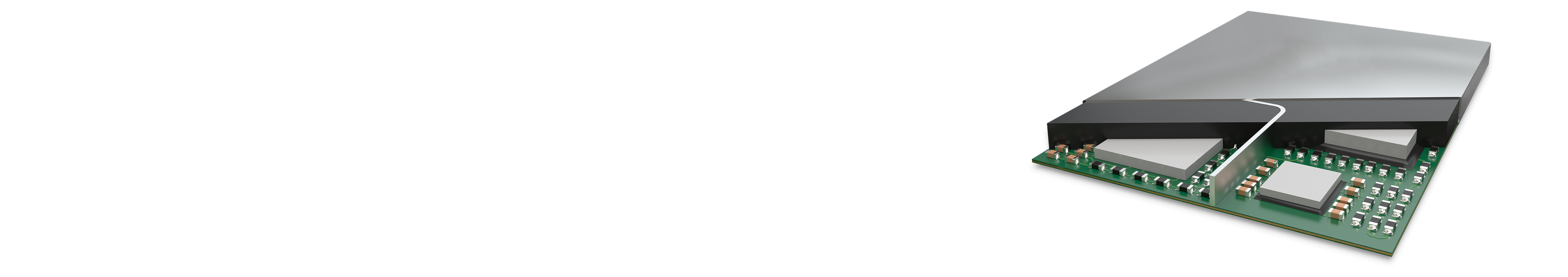
Silver and Semi sintering die attach pastes
Sintering and Semi sintering die attach adhesives for semiconductor packaging
- Home

- Products
- Die Attach Materials
- Sintering and Semi Sintering Pastes
Sintering and Semi Sintering Pastes
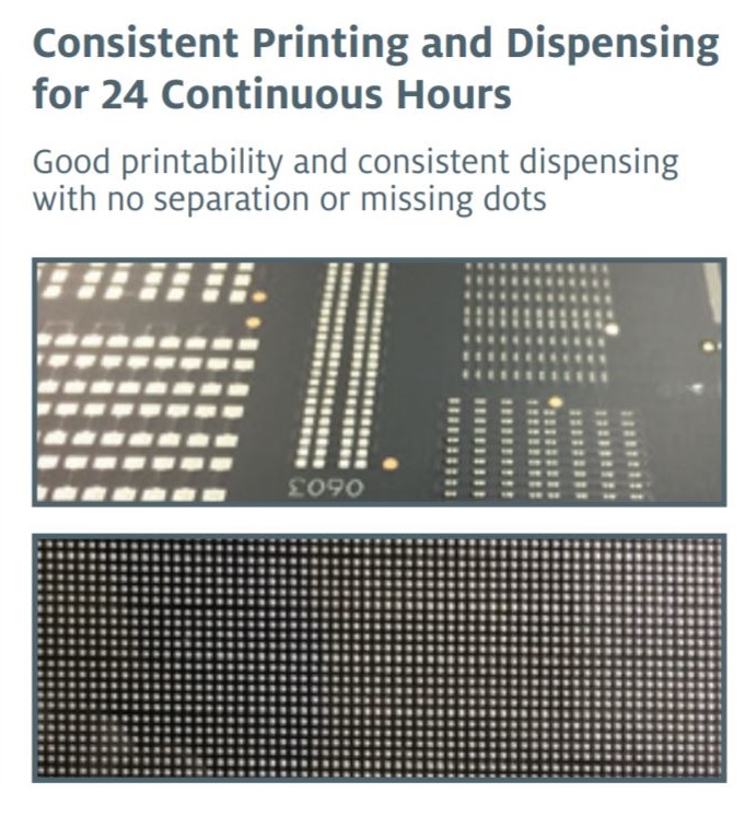
Semi sintering die attach pastes are resin based drop in solutions, identical to standard die attach paste applications but without the need for high pressure and temperature for sintering. They are characterised by excellent workability, allowing for consistent dispensing for 24 continuous hours, without silver settling or separation. Lead-free die attach materials that offer simplified processing, robust reliability and best-in-class thermal and electrical performance for high power density semiconductor packages.
Sintering products on the other hand have different process requirements and are solvent based, making them a possible but not ideal option for semiconductor packages. Their thermal capabilities are through the roof but the fact that they contain solvent (that could potentially popcorn) makes them struggle with MSL requirements. They are stencil printable, mainly targeted towards High thermal package applications that use metalized back side die, Ag or Au coated substrates or other metalized leadframes.


LOCTITE ABLESTIK SSP 2020
- High thermal conductivity
- High electrical conductivity
- High die shear strength
- 12 weeks
Product Selector Guide
| Product | Description | Viscosity | Thixotropic index | Shear strength 2x2mm @260°C | Tensile modulus @25°C | Glass transition temperature (°C) | CTE a1 | CTE a2 | Key attributes |
|---|---|---|---|---|---|---|---|---|---|
| Loctite Ablestik 8068TB | Ag-filled semi sintering die attach adhesive | 11,500 | 5.5 | 6.5 | 12,500 | 25 | 25 | 103 | Good workability High thermal stability Solder replacement |
| Loctite Ablestik 8068TA | Ag-filled semi sintering die attach adhesive | 9,000 | 6 | 7.3 | 11,800 | - | 54 | - | Excellent workability Dispensable Printable |
| Loctite Ablestik 8068TI | High Ag-filled semi sintering die attach adhesive | 13,000 | 5.5 | 9.4 | 24,000 | - | - | - | High thermal packages High Ag content >165 W/mK |
| Loctite Ablestik 8068TD | Ag-filled semi sintering die attach adhesive | 11,000 | 6.8 | 9.0 | 7,400 | - | - | - | Non-metallized Backside >50 W/mK |
| Loctite Ablestik SSP2020 | Ag-filled Pure sintering die-attach | 19,000 | 5 | - | 12,490 | - | - | - | High thermal packages >100 W/mK |
Frequently Asked Questions
TDS says that I should cure in N2 Oven. Can I cure in a conventional one?
Many customers prefer to cure in Nitrogen, to protect components from oxidation. However,our testing data packages state that cure in Air or Nitrogen is mostly OK. Justification data is rather mathematical, but it tends to show that die shear strength is not significantly affected by the curing atmosphere.
- Looking at all test results so far, we believe that our hybrid sintering materials can sinter well under both AIR and N2 atmosphere. We see some variation depending on the application which can go both ways.
- The O2 in AIR will typically support the sintering process by decomposing the lubricant barrier on the Ag filler at higher temperature faster and this way accelerate the Ag particles to contact and diffuse.
- The flow of N2 will help to remove the volatiles in the system, such as solvent and low molecular resins, and this way support the sintering process. To decompose the lubricant under N2 condition may require longer sintering process to achieve full sintering.
The main reason for using cure under Nitrogen is to prevent the Cu lead frame from oxidizing more under high temperatures. Practically, this has nothing to do with our semi-sintering materials as long as they use Ag of Au/PPF plating on die pad.
Is Henkel also working on sintering materials which will sinter under pressure, like in Power Modules ?
The first sintering material that we developed ~10 years ago was SSP 2020 based on solvent based pure sintering. This can be used with and without pressure depending on the application requirements.
Being a specialty chemical supplier with leading position in high speed semiconductor die attach, Henkel continues to develop HYBRID based materials without the need for pressure. This may also include integrated power modules with larger die size on DBC for instance, to replace pressure assisted sintering.
What effects Gan on SiN and the substrate will have on the process?
Silicon Nitride is an alternative to Silicon. The wafer / chip is normally fabricated from Silicon Nitride. This is mechanically fairly similar to silicon (it’s a bit harder & more brittle), so die attach that works with silicon is typically good on SiN.
GaN (Gallium Nitride) is a semiconductor layer that is grown on top of a silicon or SiN wafer / chip surface. So for die attach it is similar to attaching a Si or SiN chip.
Semi sintering materials need a layer of Ag or Au on both the chip & the substrate to give a good bond. This means that you should have a noble Back side metallization (BSM) on the die for the sintering to take effect. Bare Cu on the substrate can be OK for some “non-critical” applications but not recommended.
Will curing of a semi-sintering paste work in a vacuum oven?
Short answer is, "probably, but we cannot recommend this". We don't except benefits for sintering semiconductor die attach pastes.
Long answer is going to be, well, long so we change our format to take the entire column span... Let's begin by saying that we have no specific data about curing semi-sinter adhesives in vacuum and this is mostly anecdotal experience:
- The “chemistry” of the adhesive resin does not require oxygen (or any other gas) to be present during the cure process.
- There is a belief that oxygen may help to remove the coatings on the fine Ag filler, and therefore promote efficient sintering. Early sintering products were quite sensitive to this effect. Our latest formulations show little dependency on oxygen content, so this mechanism may now be “history”.
- The solvent (about 4% by weight) needs to be removed in a controlled way, to eliminate the risk of void formation. A high vacuum will cause the solvent to evaporate quickly, and it could even boil in some circumstances.
- Some components in the epoxy resin can evaporate in the early stages of cure (before they have a chance to react & cross-link). This evaporation will be accelerated in a vacuum so the end properties of the adhesive may be changed. This may not be significant, but we have no data – therefore we recommend to start with curing at normal pressures, and then evaluate the effects of vacuum carefully.
The vacuum oven will indeed improve (reduce) potential voiding issues, but this is typically not perceived as a problem for resin based ABP 8068TB product types. For solvent based pure sintering materials like SSP 2020 this can be an advantage BUT these products are typically not suitable for semiconductor die attach passing certain MSL levels, so this is irrelevant.
Learn More
Semi Sintering Die Attach Pastes
Smaller, higher functioning devices within applications in various market sectors are increasing power densities and driving the need for more effective heat dissipation. While thermal interface materials offer this capability at the board and component level, more user-friendly and effective thermal management solutions are needed at the die level.
High thermal semi-sintering die attach materials enable robust package-level sintering and overcome the regulatory challenges of solder, thermal conductivity limitations of traditional die attach materials, and processability complexities of pure sintering pastes. The LOCTITE® ABLESTIK® ABP 8068T portfolio features high thermal, semi-sintering die attach pastes that offer simplified processing, and best-in-class thermal and electrical performance with robust reliability for today’s high power density devices. They also offer an open time of up to two hours and void-free bond lines, promoting high reliability and manufacturing flexibility.
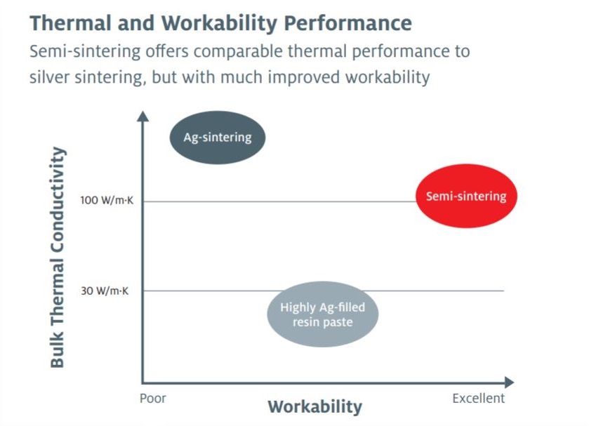
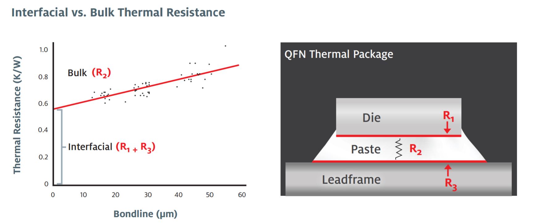
Silver filled High thermal pastes,allow for excellent dispensing, but cannot achieve ultra-high thermal conductivity due to limited filler loading and conductivity only from metal to metal contact; there is no interfacial metallic formation.
Pure sintering pastes with no resin in the matrix are highly silver-filled pastes and can achieve ultra-high thermal conductivity but have limitations and need special processing such as high termperature and high pressure to eliminate porosity or voiding.
Semi-sintering, or hybrid sintering is a combination of sintered silver and a resin system. Processing is similar to that of standard die attach pastes with robust reliability, best-in-class electrical and thermal performance, and high-volume manufacturing capability.
Semi-Sintering Die Attach Paste Benefits
- Drop-in solution identical to standard die attach paste applications without any need for high pressure and temperature for sintering
- Consistent needle dispensing for 24 continuous hours and stable for up to 6 hours of stencil open time
- Bulk thermal conductivity up to 110 W/m·K
- High die shear strength on various substrate finishes, including silver, copper, nickel-palladium-gold and gold
- Die size range up to 5 mm x 5 mm
'Next Gen' Hybrind Ag Sintering
The Next generation hybrid sintering increases bulk sintering and intermetallic diffusion on both Ag and Au surface with thermal conductivity reaching 165W/km. For non-metallized die backside, an increase in resin content with thermal conductivity reaching 50W/mk. Both variants passed automotove reliability up to 3mm x 3mm die size.