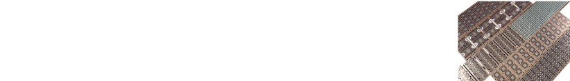
Leadframes for IC Semiconductor Assembly
Cu, Ag, NiPd & PPF plated Leadframes
Leadframes
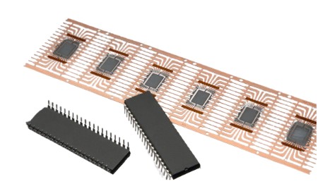
Caplinq provides a large variety of Leadframes for Semiconductor package assembly, ranging from Bare Copper (Cu) to Silver(Ag), NiPd (Nickel Palladium) and PPF (Nickel Palladium Gold) platings.
We can manufacture Pre plated custom leadframes for all types of packages including but not limited to QFN, PLCC, QFP, HDL, PDIP, TSOP, SOIC, SQP, DIP, TO220, FDIP, SIP and SOP. You name it, we make it. We can also explore options for thinner and higher thermal dissipation packages.By leveraging a smart and adjustable production process we can honor low volume orders for IC package manufacturers that want to experiment with new and alternative packaging approaches.
Additionally, epoxy molding compound manufacturers and companies that might want to test their Molding compounds in-house can take advantage of our flexible and adjustable Pull tab adhesion leadframes. Our current range includes one of the most popular strip designs with 8 units per strip in 4 different platings. We can manufacture and plate your custom designs so reach out to us for a quotation.
 From
From
$2.36
PTLF | Pull Tab Adhesion Leadframe
- Pull tab adhesion design
- 8 units per strip
- Various platings
- 4 weeks
Frequently Asked Questions
Can we get a different roughness of Cu on the lead frame surface?
Yes, we provide AE treatment, this is a Cu roughening technology and has been widely used in the industry for decades already.
Does Caplinq have the capability of locking holes on the leadframe ?
Yes, locking hole can be done by etching.
Can Caplinq do injection molding at engineering basis to form 8x8 PDFN parts ?
No, we do not offer injection molding services.
What are the caplinq leadtimes ?
Our FAI lead time is typically 4 to 8 weeks, depending on the package. And we normally offer 100 strips FOC samples to our customers with the NRE charge.
What are the key considerations for selecting the right leadframe material for a specific semiconductor package?
When choosing the leadframe material for a semiconductor package, consider these key points:
- Electrical Conductivity: Opt for materials that conduct electricity well.
- Thermal Properties: Ensure the material can handle heat generated by the chip.
- Corrosion Resistance: Look for materials that resist rust or damage to ensure long-term reliability
- Wire Bonding Compatibility: Consider how well the material works with wire bonding (connecting the chip) that affect the electrical performance.
- Environmental Factors: Think about where the package will be used (humidity, temperature, etc.).
Remember, good leadframe material ensures reliable electronics.
Is leadframe surface roughness a main contributor for mold flash?
No. Mold flash is mainly contributed by the following factors; (1) Mold-related factors such as parting line mismatch, improper venting and inadequate sprue bushing support (2) Process-related factors such as transfer pressure, mold temperature, transfer speed, cure time, and cleaning and (3) Resin type and viscosity. Surface roughness however, may contribute to mold flash occurrence on semiconductor devices due to rougher surfaces which tend to have higher risks of mold flash formation due to increased entrapment points for the resin.
To have continuity on the roughness values:
- Low Roughness (less than 10 microns)
- Medium Roughness (10-50 microns)
- High Roughness (above 50 microns)
Remember, achieving good mold flash control relies on a holistic approach that optimizes mold design, process parameters, resin material selection as well as leadframe surface roughness. By carefully considering and optimizing all these factors, you can achieve the best possible results in your specific transfer molding application.
Learn More
Semiconductor Leadframes: The Unsung Heroes of Electronics
Semiconductor leadframes are the metal skeletons behind our electronic devices. They serve two crucial functions:
- Connecting Chips to the World: Imagine them as tiny bridges with metal "legs" extending outwards. These legs, called leads, provide the electrical pathways for the tiny circuitry inside the chip to connect with the larger wires and components on a circuit board. Thin wires called bond wires bridge the gap between the chip's pins and the leadframe's bond pads on each leg.
- Offering Support and Protection: Leadframes not only carry signals but also act as platforms for holding and protecting the delicate silicon chip. They prevent damage during assembly and handling, ensuring the chip functions reliably.
- Heat dissipation: Leadframes are designed to help dissipate heat generated by the chip, ensuring its optimal performance and longevity.
- Cost-effectiveness: Compared to other packaging methods, leadframes offer a cost-effective solution for mass production of electronic devices.
What are they?
Benefits of Leadframe Roughening
Semiconductor leadframes typically need some degree of roughening for optimal performance and reliability in semiconductor packaging.
- Improved Adhesion: A roughened surface provides more "grip" for the molding compound and solder, minimizing the risk of delamination and ensuring strong electrical and mechanical connections.
- Enhanced Solderability: Roughness increases the wettability of the leadframe surface, leading to a more uniform and reliable solder joint with bonding wires and other components. This improves electrical conductivity and thermal transfer, enhancing device performance.
- Reduced Tin Whisker Growth: Tin whiskers are microscopic hair-like growths on lead surfaces that can cause electrical shorts and device failures. Certain roughening techniques, like grit blasting, can help suppress whisker growth.
Challenges and trends in semiconductor leadframe technology
The world of leadframe technology faces exciting challenges and trends, constantly pushing the boundaries of miniaturization, performance, and sustainability.
- Miniaturization: As chip sizes become smaller, accommodating them on leadframes while maintaining enough lead density and ensuring thermal management becomes increasingly difficult. Developing thinner and lighter leadframes with innovative lead configurations is crucial.
- Heat dissipation: The ever-growing heat generation of high-performance chips demands better heat dissipation solutions. Exploring materials with higher thermal conductivity and optimizing leadframe design for efficient heat transfer are key concerns.
- Cost-effectiveness: Balancing advanced features with affordability remains a challenge. Finding cost-effective materials and manufacturing processes without compromising performance is essential for mass production.
- Sustainability: Lead-based solder used in traditional leadframes raises environmental concerns. Developing lead-free alternatives and minimizing resource consumption are important ethical considerations.
- Reliability and testing: As leadframes become more complex and miniaturized, ensuring their reliability and developing accurate testing methods become critical. New testing approaches and standards are needed to keep pace with technological advancements.