Sensors
MEMS, Cameras, Fingerprints
- Home

- Electronics Assembly
- Sensors
- Camera Image Sensors
Camera Image Sensors
The evolution of cameras marks one of the most fascinating technological journeys in modern history. From the large box-type camera obscura during the 17th century to the pocket-sized cameras embedded into our cellular phones in the 21st century. Cameras have shrank and are still shrinking at an exponential rate. A key player in this transformation? Image sensors.
Image sensors are critical semiconductor devices that enable digital imaging by converting light into electrical signals. They function as the "electronic eye" in a wide range of devices, from smartphones and digital cameras to security systems and automotive driver assistance technologies. At the core of these sensors is an array of photodiodes, tiny light-sensitive elements arranged in a two-dimensional grid. When light photons strike the photodiodes, they generate electric charges proportional to the light's intensity. These charges are then amplified and converted into digital signals to form images.
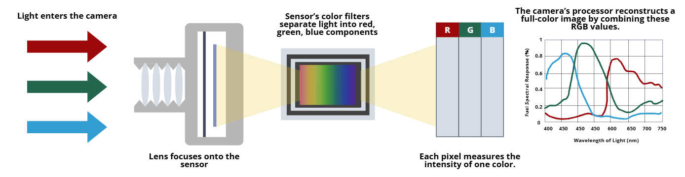
The figure illustrates how color image sensors capture and process light to form digital images. Incoming light composed of red, green, and blue wavelengths passes through the camera lens and onto the sensor surface. A color filter array positioned above the sensor divides the light into its respective RGB components, enabling each pixel to record the intensity of one color channel. These signals are then combined and processed to reconstruct a full-color image. The spectral response curves show the sensitivity of each color filter across the visible wavelength range, highlighting how red, green, and blue channels respond most strongly near 600–650 nm, 550 nm, and 450 nm, respectively. This will then become the data used to generate the output image.
Two Major Types of Image Sensors
There are two primary types of image sensors: charge-coupled devices (CCD) and complementary metal-oxide-semiconductor (CMOS) sensors, both born from developments in the late 1960s. CCD sensors move electrical charge across the chip in a sequential manner to a single output node, making them historically preferred for high image quality due to low noise.
CMOS Image Sensors
CMOS (Complementary Metal-Oxide-Semiconductor) image sensors integrate pixel-level amplification and signal processing directly on the chip. They consume less power, offer faster readout speeds, and are easier to integrate with digital circuits—making them ideal for compact, power-sensitive aerospace imaging systems.
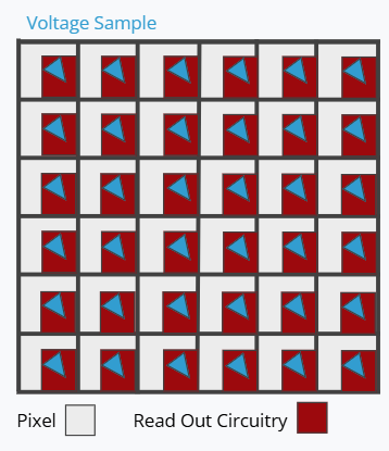
In CMOS sensors, Each pixel generates and measures its own voltage signal in response to light. The image is read electronically rather than physically shifting charge.
Most Common Use: Small satellites, UAVs, and onboard vision systems
PROs: Low power consumption; fast readout; compact integration; tolerant to vibration.
CONs: More noise than CCD; lower sensitivity in low light (though improving with technology).
USE CASES: Autonomous navigation, star tracking, real-time imaging, optical payloads in small spacecraft.
CCD Image Sensors
CCD (Charge-Coupled Device) image sensors transfer charge across the chip to a common output node, producing low-noise, high-quality images with excellent light sensitivity. They are well-suited for scientific and space observation missions demanding precision and image clarity.
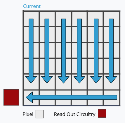
In a CCD, pixels pass electric charge (current) along the array toward the readout node. This means the image data moves physically through the chip — pixel by pixel — before it’s read out.
Most Common Use: Space telescopes, high-resolution Earth observation, deep-space imaging
PROs: Superior image quality; high sensitivity; low noise; proven radiation performance.
CONs: Higher power consumption; slower readout; more complex drive electronics.
USE CASES: Astronomy imaging, scientific payloads, high-resolution Earth observation, radiation-hardened cameras.
Fabrication and Assembly of CCD and CMOS Image Sensors
Image sensors—whether CCD (Charge-Coupled Device) or CMOS (Complementary Metal-Oxide-Semiconductor)—are among the most complex semiconductor components in modern electronics. Both technologies transform light into electrical signals, but their fabrication and assembly processes reflect distinct design philosophies that influence performance, power consumption, and application suitability.
Shared Foundations
Both CCD and CMOS sensors are built on high-purity silicon wafers, using a combination of photolithography, doping, and thin-film deposition to define their intricate pixel structures and readout circuits. The overall goal in both processes is to create uniform, light-sensitive photodiodes arranged in a precise pixel grid, and to integrate optical layers that enhance light collection efficiency.
Up to this point, both CCD and CMOS follow similar semiconductor fabrication principles—but they diverge sharply in how signals are processed, read, and packaged.
Fabrication Differences
The fabrication of CCD and CMOS image sensors both rely on silicon wafer processing, yet they diverge significantly in structure, integration method, and manufacturing complexity. CCDs employ specialized charge-transfer structures, while CMOS sensors leverage the same technology used in logic and memory ICs.
| Feature | CCD | CMOS |
|---|---|---|
| Process Base | Specialized Large-Scale Integration (LSI) with optimized charge transfer gates | Standard CMOS LSI compatible with logic Integrated Circuit (IC) fabs. |
| Pixel Structure | Photodiode + charge-transfer channel | Photodiode + transistors for in-pixel amplification |
| Readout Scheme | Charge transferred sequentially to common output node | Parallel pixel-level readout through metal lines |
| Isolation | Local Oxidation of Silicon (LOCOS) and channel-stop diffusion | Deep n-well and Shallow Trench Isolation (STI) isolation |
| Integration | Separate imaging die (often hybridized) | Monolithic integration with signal processing circuits |
| Cost and Complexity | Expensive, wafer yield sensitive | Lower cost, uses mainstream fabs |
In short, CCDs prioritize high-quality charge handling via complex analog processing, while CMOS sensors achieve speed, integration, and low cost through digital-friendly semiconductor processes.
Assembly and Packaging
Once fabricated, both CCD and CMOS wafers are diced into individual dies and undergo assembly to transform them into usable sensor modules.
Dicing and Die Attach
Individual dies are cut from the wafer and mounted on a package substrate.
Electrical Interconnection
Achieved through wire bonding or flip-chip attachment, connecting the die to external leads or PCBs.
Encapsulation and Sealing
The sensor is protected from moisture and contaminants, often under a glass or ceramic cover window.
Optical Alignment
Lenses, filters, and other optical components are precisely aligned to the pixel arra
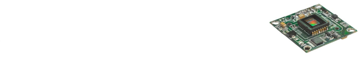
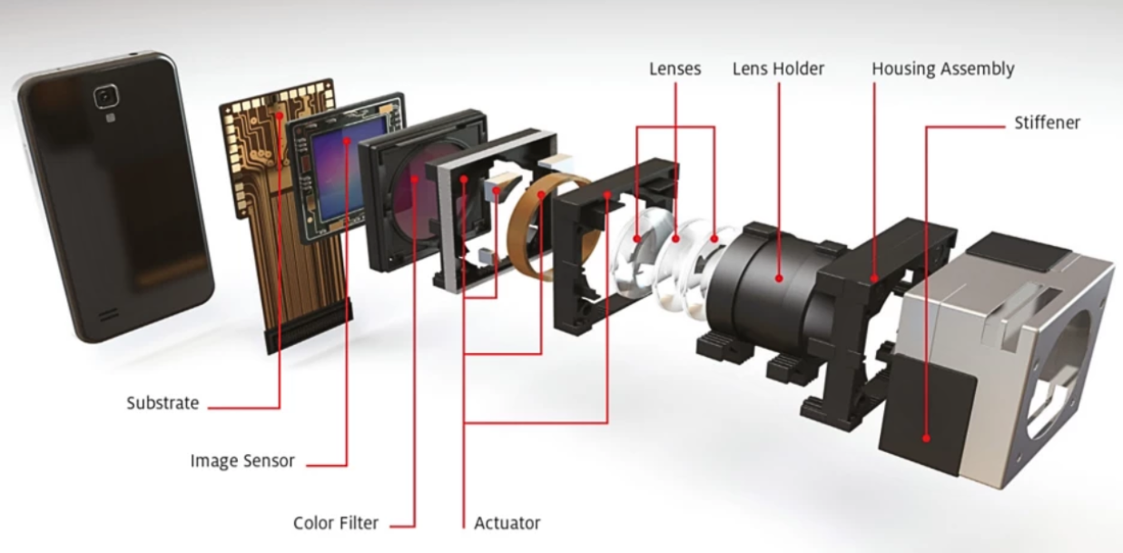
Once fabrication is complete, the image sensor is integrated into the camera module. It is precisely mounted and aligned with the lens, lens holder, and housing assembly to ensure accurate optical alignment, consistent image quality, and mechanical stability. This meticulous assembly process is critical for achieving reliable sensor performance and long-term durability in the final camera system. Learn more about camera module assembly here.
Materials for Image Sensor Packaging
For CCD and CMOS image sensors, packaging materials must offer low outgassing, fast or low-temperature cure, and excellent adhesion on engineering plastics (such as LCP and PC), ceramics, and metals commonly used in aerospace assemblies.
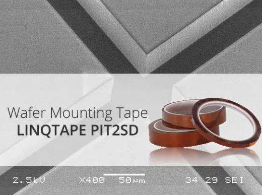
Polyimide Tapes for Image Sensor Fabrication
In image sensor manufacturing, precision and cleanliness are critical at every stage — from wafer processing to final packaging. Polyimide tapes play a vital role in protecting delicate wafer surfaces, die edges, and optical components during photolithography, etching, dicing, and metallization steps.
Recommended Polyimide Tapes for Image Sensor Fabrication
For aerospace memory die attach, we want:
- High thermal stability to withstand photolithography, etching, and metallization steps
- Strong, residue-free adhesion on wafer surfaces and frames during high-temperature processing
- Low outgassing and chemical resistance for cleanroom and optical environments
- Dimensional stability to ensure precise alignment and masking in photolithography
- Easy removal without contaminating sensitive sensor structures
Caplinq’s LINQTAPE™ PIT-Series polyimide tapes are engineered to deliver exceptional thermal stability, chemical resistance, and low outgassing performance required in cleanroom semiconductor environments. Available with both silicone and low-outgassing acrylic adhesives, these tapes maintain strong adhesion on a variety of substrates while ensuring residue-free removal after high-temperature exposure.
| Product | Film / Tape Description | Key Properties & Why They Matter for Photolithography |
|---|---|---|
| PIT1A-LO | 1 mil (~25 µm) polyimide film with low-outgassing acrylic adhesive. |
|
| PIT2A-LO | 2 mil (~50 µm) polyimide film with low-outgassing acrylic adhesive. |
|
| PIT1S | 1 mil polyimide film with silicone adhesive. |
|
| PIT2S | 2 mil polyimide film with silicone adhesive. |
|
| PIT1S-RL | 1 mil polyimide tape with silicone adhesive on release liner. |
|
Sensor Die Attach to Substrate
Adhesives for die attach applications must combine strong adhesion with low outgassing, fast curing, and excellent environmental stability. These materials ensure reliable bonding between sensor die and substrate even under challenging temperature conditions.
| Key Requirements | Recommended Products |
|---|---|
| • High adhesion on various substrates • Fast cure from 80 °C to 175 °C • Low moisture absorption and outgassing • Excellent impact resistance • −40 °C to 130 °C operating range • Low halogen content | LOCTITE ABLESTIK QMI 536NB: Low stress, low resin bleed, low moisture absorption, fast cure. LOCTITE ABLESTIK ABP 2035SC(R): High adhesion, low temperature cure, suitable for small–medium die size. LOCTITE ABLESTIK ABP 6892: Transparent, low stress for ultra-thin die, low temperature cure. |
Adhesives Lens Holder, Lens Barrel, and IR Filter Bonding
Optical bonding materials must adhere to plastics like PC and LCP while curing quickly at low temperatures to prevent distortion. They ensure precise alignment, long-term stability, and resistance to mechanical or thermal stress.
Recommended Adhesives for Image Sensor Packaging
For Image sensor fabrication and assembly, we want:
- Low halogen content
- Strong, residue-free adhesion to diverse substrates (PC, LCP, etc.)
- Low temperature cure <100 °C
- Fast cure <60 mins
- Low operating range of between−40 °C to 130 °C
| Recommended Products | Properties |
|---|---|
| LOCTITE ABLESTIK 8387B: | High adhesion, medium viscosity, low temperature cure. |
| LOCTITE ABLESTIK ABP 2035SC(R): | High adhesion, low temperature cure |
| LOCTITE ABLESTIK ABP 6892: | Transparent, low stress for thin bond line, low temperature cure. |
| LOCTITE 3220 / 3220WH: | High adhesion, low viscosity, low temperature cure (available in black or white). |
UV Cure Adhesives for Active Alignment
Dual-cure and UV-curable adhesives enable rapid, precision assembly of optical components during active alignment. Their low viscosity, fast curing, and thermal stability make them ideal for automated high-speed camera module manufacturing.
| Recommended Products | Key Features |
|---|---|
| LOCTITE ECCOBOND OGR-150THTG LOCTITE 3217 LOCTITE 3707 LOCTITE 3103 LOCTITE 3703 | Low viscosity UV + low-temp cure adhesive High viscosity, stencil printable, dual cure Medium viscosity, UV + thermal edge bonding UV-only cure, medium viscosity Thixotropic viscosity for anti-migration |
Image Sensor Chip Scale Package (CSP) Underfill
Underfill materials protect solder bumps and interconnects from thermal cycling and mechanical stress. High-Tg and low-CTE formulations ensure long-term stability and reliability in compact image sensor packages.
Recommended Adhesives for Image Sensor Fabrication
For Image sensor fabrication and assembly, we want:
- Low halogen content
- Strong, residue-free adhesion to diverse substrates (PC, LCP, etc.)
- Low temperature cure <100 °C
- Fast cure <60 mins
- Low operating range of between−40 °C to 130 °C
| Key Requirements | Recommended Products |
|---|---|
| • Bump protection across various substrates • High Tg, low CTE for minimal stress • Excellent impact and thermal cycling resistance • −55 °C to 150 °C temperature cycling • Low halogen | LOCTITE ECCOBOND FP4531: High Tg (~160 °C), low CTE (~28 ppm), snap-cure (7 min @ 160 °C). LOCTITE ECCOBOND E1216M: Automotive use, fast and lower temperature cure. LOCTITE NCP 5209: Medium viscosity, designed for high-Tg via thermal compression bonding. |
Frequently Asked Questions about Image Sensors
Why are low-outgassing materials essential in image sensor packaging?
Low-outgassing materials prevent volatile compounds from condensing on optical surfaces like microlenses and filters. Contamination at this level can degrade light transmission, increase noise, and distort color accuracy. For high-sensitivity sensors—especially those used in aerospace, automotive, or scientific imaging—adhesives and encapsulants are qualified for TML < 0.2% and CVCM ≈ 0% to maintain optical and electrical integrity over time.
How do protective coatings enhance wafer-level processing of sensors?
During wafer processing, thin protective films such as polyimide coatings or protective tapes are applied to safeguard sensor surfaces from plasma etching, metallization, and dicing damage. These coatings must have excellent chemical resistance, controlled adhesion, and residue-free removal. The trend is toward UV-release or thermoplastic protective layers that simplify post-processing removal and minimize particle generation.
As pixel densities increase, local heat buildup becomes a significant reliability concern. Materials such as thermally conductive die attach adhesives and underfills help spread and dissipate heat efficiently. Silver-filled epoxies, for instance, offer thermal conductivities up to 10 W/m·K, helping maintain consistent dark current levels and reducing hot pixel formation during continuous operation.
How are reworkable or low-temperature materials beneficial to image sensor assembly?
Optical modules often integrate multiple lenses and filters over sensitive dies that cannot tolerate high reflow temperatures. Reworkable adhesives with curing below 100–120°C enable precision alignment without thermal damage. They also allow for part replacement or repair—critical in production lines where yield optimization is key.
Learn More
Related Blogs

How Temperature Resistance of Polyimide Films and Tapes Works
Electrically Conductive Adhesives for Heat-Sensitive Electronics and Camera Modules