Semiconductor Epoxy Mold Compounds
Semiconductor grade epoxy molding compounds with high electrical stability
- Home

- Products
- Molding Compounds
- Semiconductor Epoxy Mold Compounds
Semiconductor Epoxy Mold Compounds
Semiconductor molding compounds are fine filled, electrically stable compounds, ideal for the miniaturised semiconductor packaging requirements. They have small filler sizes, great spiral flow and can be electrically stable at high temperatures.
Epoxy molding compounds that are graded for semiconductor use are CTE matched to common die substrates and are made with nano packages in mind. They cover and protect the die and the wirebonding while also passing the most stringent moisture and temperature tests.
Excellent electrical stability is desired for epoxy molding compounds used in the encapsulation of high power, discrete semiconductors applications that also operate a high temperatures.These molding compounds tend to have the lowest ionic content, the highest dielectric strength, the most stable dielectrics and the lowest ionic conductivity over the widest possible temperature range.


LINQSOL EMC-7560 | Black Epoxy Mold Compound
- High Glass Transition Temperature (205 °C)
- Designed for high voltage, high power discrete packages
- New Epoxy System To Pass HTRB Tests
- 8 weeks

Hysol GR720 | Black Epoxy Mold Compound
- High reliability
- Green and halogen-free
- Designed for SOT applications
- 12 weeks

Hysol KL1000-3LX | Black Epoxy Mold Compound
- High reliability
- High moldability
- Decreased cost-of-use
- 12 weeks

LINQSOL EMC-7535 | Black Epoxy Mold Compound
- Green molding compound
- Designed for high-power TO packages
- High Tg, low water absorption, low modulus, and excellent thermal stability
- 8 weeks

LINQSOL EMC-7142 | Black Epoxy Mold Compound
- Green epoxy molding compound
- Designed for SOP and QFP
- Low water absorption, low stress, and excellent moldability
- 8 weeks

LINQSOL EMC-7535MF | Black Epoxy Mold Compound
- Green molding compound
- Designed for high-power TO packages
- High Tg, low water absorption, low modulus, and excellent thermal stability
- 12 weeks

Hysol GR350HT | Black Epoxy Mold Compound
- High Thermal Conductivity GR30
- Designed for TO92 and TO220 packages
- Excellent reliability under high temperature and bias
- 16 weeks

LINQSOL EMC-6043 | Black Epoxy Mold Compound
- High Spiral flow
- Designed for SOT and Modules
- Low stress and Low Moisture Absorption
- 12 weeks

LINQSOL EMC-9012 | Black Epoxy Mold Compound
- Green epoxy molding compound
- Designed for Ball Grid Array (BGA) and Land Grid Array (LGA) packages.
- Ultra low water absorption, low stress, and excellent reliability performance.
- 12 weeks

Hysol GR910-K | Black Epoxy Mold Compound
- Halogen free
- High fluidity to avoid W/S issue
- Designed for BGA/LGA
- 12 weeks

LINQSOL EMC-9131 | Black Epoxy Mold Compound
- High Spiral flow
- Designed for SOT and Modules
- Low stress and Low Moisture Absorption
- 16 weeks

Hysol GR700 | Black Epoxy Mold Compound
- Low stress
- For high power devices
- Good electrical performance
- 12 weeks

LINQSOL EMC-5013 | Thermally conductive Epoxy Mold Compound
- Green epoxy molding compound
- Thermally conductive molding compound
- Designed for transistor outline (TO) and fullpack power packages
- 12 weeks

LINQSOL EMC-9023 | Epoxy Mold Underfill
- Green epoxy molding compound
- Epoxy mold undefill
- Designed for FCBGA, FCCSP, SiP
- 12 weeks

LINQSOL EMC-G135 | Thermally Conductive Epoxy Mold Compound
- Green epoxy molding compound
- Low cost thermally conductive molding compound
- Designed for rectifier bridges and SMX packages
- 2 weeks

LINQSOL EMC-1533 | Black Epoxy Molding Compound
- Green molding compound
- Designed for transistor outline (TO) and double decawatt (D2PAK) packages
- Excellent workability, low water absorption, low modulus, and excellent thermal stability
- 2 weeks

LINQSOL EMC-9012H | Black Epoxy Mold Compound
- Green epoxy molding compound
- Designed for Ball Grid Array (BGA) packages and Quad Flat No Leads (QFN) Packages
- High glass transition temperature, low stress, and excellent reliability performance
- 2 weeks

LINQSOL EMC-G833 | Black Epoxy Mold Compound
- Green epoxy molding compound
- Designed for Quad Flat No Leads(QFN), Quad Flat (QFP) packages and DFN Packages
- Excellent reliability performance
- 12 weeks

LINQSOL EMC-G833R | Black Epoxy Mold Compound
- Green epoxy molding compound
- Designed for Quad Flat No Leads(QFN) and Quad Flat (QFP) packages
- Excellent reliability performance (MSL 1)
- 12 weeks

Hysol GR910-LB| Black Epoxy Mold Compound
- Halogen free
- High fluidity to avoid W/S issue
- Designed for BGA/LGA
- 2 weeks

EMC-G274 | Epoxy Molding Compound for Photocouplers
- Good moldability
- Designed for photocoupler / optocoupler devices
- Excellent mechanical integrity
- 12 weeks


EMC-G845 | Black Epoxy Molding Compound
- Green epoxy molding compound
- Designed for QFN & QFP packages
- Satisfies JEDEC MSL 3 reliability
- 12 weeks

EMC-G836 | Epoxy Molding Compound
- For QFN & QFP packages
- Meets JEDEC MSL 3 reliability requirements
- High spiral flow
- 12 weeks


 Black Epoxy Mold Compound")


Product Selector Guide
▶ EMC for Laminated Integrated Circuits
▶ EMC for Passive Components
▶ EMC for Optocouplers
Notes: Values are compiled from available datasheets and may be typical unless otherwise stated.
| Product | Key Feature | Package / Application |
|---|---|---|
| GR30 | Excellent fillability to fine gap; Good anti-ATF oil performance; Suitable for rotor transfer process | Permanent Magnet Synchronous Motor (PMSM) |
| GR50HT | Excellent workability; Suitable for end-pin protect coating | Permanent Magnet Synchronous Motor (PMSM) |
| GR710 | Ultrathin insulation coating; Stronger adhesion; Suitable for wholly packing stator | Permanent Magnet Synchronous Motor (PMSM) |
| GR510-HP | Higher mechanical strength; CTI level 0 | Electromagnetic Valve |
| GR710 | Excellent workability; Suitable for wholly packing application | Small Motor |
| GR50HT | Fast curing; Higher thermal conductivity; CTI level 0 | Doorhandle Sensor |
| Product | Thermal Conductivity | Package focus | Notes |
|---|---|---|---|
| Hysol GR30HT | 1.9 W/mK | TO92, TO3P, TO220, TO247 power devices | High-thermal-conductivity GR30 variant. Distributor sources indicate it has been superseded by GR350HT. |
| Hysol GR350HT | 1.6 W/mK | TO92, TO3P, TO220, TO247 power devices | Current GR30-derived high-thermal-conductivity grade for TO power packages; positioned to support high-temperature and bias reliability. |
| Hysol GR60PT | 1.7 W/mK | IPM, full-pack type IPM, substrate-type IPM | Positioned as a more cost-efficient option for power module encapsulation. |
| Hysol GR60HT | 2.2 W/mK | IPM, full-pack type IPM, substrate-type IPM | Enhanced moisture resistance and broader adhesion compatibility with Cu, Au, and Ni finishes compared to standard GR60 grades. |
| Hysol GR600 / GR600‑P1 | 1.41 W/mK | TO251 (IPAK), TO252 (DPAK), TO263 (D2PAK), TO220 | Power-discrete EMC focused on DPAK and D2PAK-class packages, with formulations designed to support MSL1 qualification and improved thermal cycling performance. |
| Hysol GR730HT | 3.2 W/mK | PSIP, TO applications, TO252 | High-thermal-conductivity, halogen-free grade for Power Supply in Package (PSIP) and TO-type power packages. |
| LINQSOL EMC‑G135 | 1.7 W/mK | Rectifier bridges, SMX | Low-cost thermally conductive EMC for bridge packages such as GBU, KBJ, and GBS. |
| LINQSOL EMC‑5013 | 2.3 W/mK | TO220F, TO3PF, full-pack power packages | Thermally conductive EMC for TO and full-pack power devices, with published thermal conductivity exceeding 2 W/mK. |
| LINQSOL EMC‑G375 | Up to 3.3 W/mK | TO‑3P, TO‑220, TO‑126, bridge rectifier, high‑power semiconductor packages | High-thermal-conductivity grade aimed at full-pack TO power packages, bridge rectifiers, and other high-power semiconductor applications. |
| Product Name | Key Properties | |||||||||
|---|---|---|---|---|---|---|---|---|---|---|
| Color | Specific Gravity | Glass Transition Temperature (Tg), °C | CTE, Alpha 1 ppm/°C | CTE, Alpha 2 ppm/°C | Moisture Absorption | Ionic Content Na+/K+/Cl- ppm | Spiral Flow | Thermal Conductivity (W/mK) | Dielectric Constant | |
| MG15F-35A | Black | 1.82 | 191 | 21 | 63 | 0.64% | 4/1/7 | 28" | 0.7 | 3.5 |
| MG21F-02 | Black | 1.81 | 179 | 21 | 62 | 0.61% | 4/1/6 | 26" | 0.7 | 3.6 |
| MG33F-0520 | Gold | 1.87 | 170 | 20 | 70 | - | 1.5/-/2 | 25" | - | 4.3 |
| MG33F-0661 | Gold | 1.81 | 164 | 18 | 60 | 0.42% | - | 27" | 0.8 | 4.1 |
| MG57-0660 | Gold | 1.82 | 168 | 21 | 70 | 0.42% | - | 30" | - | 4.2 |
| MG33F-0602 | Black | 1.80 | 162 | 22 | 65 | - | 2/-/7 | 43" | - | 3.9 |
Frequently Asked Questions
What exactly is an HTRB test?
A "High Temperature Reverse Bias" test is a common reliability test that exposes the power devices (and hence the EMC) to the "worst case scenario" under which it must perform and not fail. During the HTRB test, the power semiconductor devices are stressed at the maximum rated reverse breakdown voltage at a temperature close to their maximum rated junction temperature (Tj max) over a defined period of time. As such, a HTRB cannot be completely understood until the variables of voltage, temperature and time are defined.
What is the ionic content in epoxy mold compound that causes semiconductor device failure?
There are four main elements that should be minimized in epoxy molding compounds. There are Chlorine (Cl-), Sodium (Na+), Fluorine (F-) and Potassium (K+), where chlorine and sodium are the most important. All the ionic content shoudl be kept under 20ppm for each individual element and less than 5ppm is desired for Chlorine and Sodium.
What is Reverse Bias?
Basically, semiconductors allow current to flow in one direction: from the p-type (positive) to the n-type (negative). Reverse bias is applying direct current (DC) voltage to prevent current flow in a diode, transistor or similar. Wikipedia has a good desription in Reverse Bias
What is the relationship between Permittivity and Dielectric Constant?
The dielectric constant is unitless because it is actually the ratio of two permittivity values: the permittivity of the substance to the permittivity of the free space. Since the lowest possible permittivity is obtained in a vacuum, the permittivity of the substance is always higher and therefore the dielectric constant is always higher than 1.
What is Ionic Mobility?
Otherwise known as Electrical Mobility, it is the ability of charged electrons or protons to move through a substance (in this case epoxy mold compound) in response to an electric field that pulls them.
How can I decap ICs?
We could suggest the obvious mechanical methods but if you came here you probably want to preserve the integrity of the bond wires and the die. That's why, typically, customers use a Nitric or Sulfuric acid to etch away the epoxy. Though you should definitely take the necessary precautions with a hume hood, no inhalation, customers have used this successfully without damaging the wires. Here are almost 8 million words (30 fps, we did the math)
What is the maximum staging time of molded products between molding and PMC?
For EMC molded packages, one-shift maximum, often 8 hours from demold or ejection to the PMC heating start timestamp, is a typical production practice, applicable only under monitored humidity control and validated for the package/EMC.
Why immediate PMC is ideal?
Immediate PMC is ideal because WIP strips enter the oven in a tighter, more consistent condition, improving lot-to-lot consistency. Shorter waiting reduces moisture exposure and reduces cure drift before oven heating, which usually improves warpage consistency, reduces SAM delamination risk, and lowers reflow crack risk.
Does EMC formulation influence staging tolerance?
Yes, EMC formulation influences staging tolerance because EMC systems differ in cure kinetics and moisture resistance. Some EMCs continue curing faster during room-temperature holds, narrowing the staging window, while other EMCs slow moisture uptake at a given RH and time. Practical rule: staging limits should be verified per EMC and package family.
What to do when staging exceeds the limit?
When staging exceeds the limit or RH control is violated, a simple principle helps: contain, recover, verify. Containment means moving WIP strips within the defined response time into defined dry storage such as a dry cabinet at or below the site dry storage RH specification, sealed moisture barrier bag with desiccant, or an equivalent approved method. Recovery means running dry bake at 125°C for 2 to 4 hours followed by PMC at the earliest opportunity. The dry bake will remove the moisture absorbed in the package prior to PMC. Verification means applying the site excursion disposition, often focused on SAM delamination checks and warpage checks for affected lots.
Learn More
Epoxy Molding Compounds
Epoxy Molding Compounds (EMC) by their nature have very good electrical insulation properties. Epoxy Mold Compounds are often called "functional epoxies" or "high solid epoxies" because they are heavily loaded with fillers. These fillers, (typically silica, though other fillers are used for other properties such as thermal conductivity) are loaded more than 50% by weight be default. Highly filled systems have weight % filler loadings higher than 70% with "very highly filled loadings" as high as 92% filled by weight.
These highly-filled systems provide epoxy molding compounds with very good dielectric strength and a very high breakdown voltage, which themselves are good electrical insulation properties. These two values however are poor indicators of what is meant by "Good electrical stability" for EMCs
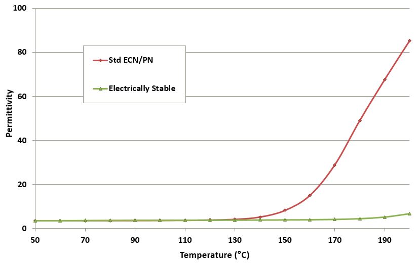
Figure 1. Low Permittivity means high electrical stability
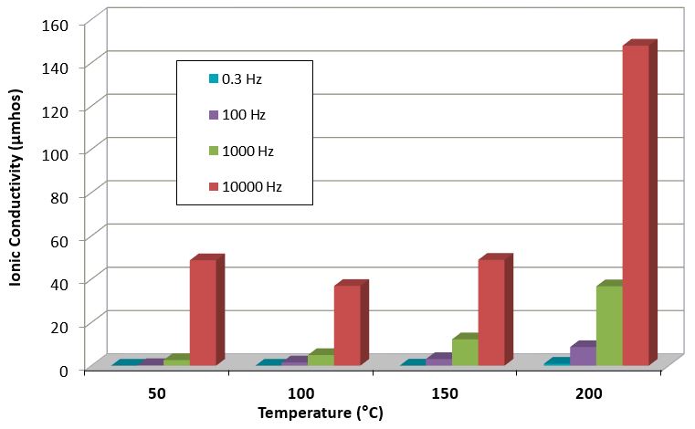
Figure 2. Ionic conductivity at different frequencies
What do we mean by good electrical stability?
Good electrical stability means that there is very little ionic movement within the epoxy mold compounds when semiconductor devices are under reverse bias at elevated temperatures. The High Temperature Reverse Bias (HTRB) reliability test is an excellent industry-developed and accepted test that tests the electrical stability of EMCs
Epoxy mold compound that are considered to have excellent electrically stability are thus those that:
- Have low ionic conductivity
- Have a low and stable permittivity at temperatures up to 200°C
- Have a high dielectric strength
- Have a stable dielectric constant over a frequency range from 1 kHz up to 1.8 GHz
What causes poor electrical stability in mold compounds?
There are two main causes of poor electrical stability in EMCs:
- The ingredients used have high ionic content
- The epoxy resin and hardner combination has high ionic conductivity
EMC subcomponents have high ionic content
Epoxy molding compounds are made up of many components including epoxy resins, curing agents, catalysts, fillers, pigments and additives. Each of these ingredients can contain ions in the form of chlorine (Cl-), Sodium (Na+), Fluorine (F-) and Potassium (K+). There are elements other than these that have ions, but these are the ions most frequently present and in the highest quantities - therefore are of the greatest interest. As you can see next to the elements listed, Chlorine and Fluorine both have negative (-) ions and Sodium and Potassium both have postitive (+) ions.
Of these four elements, the biggest culprits are Chlorine (Cl-) and Sodium (Na+). If the total ionic content is too high, or the ionic content of each of the Chlorine or Sodium is too high, then the risk of gate current leakage and device malfunction increases. In all semiconductor applications, it is prudent to have the total extractable ionic content to be less than 80ppm and the extractable content of each element to be below 20ppm. In high power semiconductor applications which operate at higher voltages and higher temperatures, it is better to have the total ionics to be below 20ppm, and of each element to be below 5ppm. As application temperature and power increase, the lower the ionic content the better.
Epoxy resin/hardner combination has high ionic conductivity
When exposed to the electric field caused by the DC voltage applied, these ions have a tendency to move. If they move too much, a gate current leakage occurs and gradually increases which ultimately leads to the device malfunction.
Different combinations of epoxy resin and hardener, will provide different ionic conductivities of the base epoxy. Specifically, as illustrated in Figure 1 below, a standard epoxy cresol novolac resin with a standard phenolic resin might have a low permittivity at lower temperatures, but quickly elevate at higher temperatures leading to gate current leakage failures for power semiconductor devices.
Formulating electrically stable Molding Compounds
Epoxy mold compound formulators can develop materials that will pass the HTRB test by developing EMCs that:
- Have low ionic content, low ionic content and low ionic mobility
- Use ion trappers
- Have low permittivity
- Use epoxy resin & hardener combinations that have the lowest ionic content and mobility
Selecting Semiconductor Mold Compounds
When looking for epoxy molding compounds that are very electrically stable, look for the following characteristics:
- Look for epoxies with a low permittivity over a wide temperature range as in Figure 1.
- Look for epoxies with a low ionic conductivity over a wide frequency range and at elevated temperatures as in Figure 2
- Look for epoxies with a stable dielectric constant up to 1.8 GHz as in Figure 3.
Choosing between granular and powder molding compound
Compression molding performance is often limited by solids handling and melt timing, not only resin chemistry. Powder EMC can dust, bridge, and contaminate equipment if fines are not controlled, while oversize particles can delay melt and create surface or appearance anomalies. Granule-shape powder EMC exists to tighten particle size distribution for stable feeding and thickness control in compression molding.
| Decision factor | Granule-shape powder EMC | Powder EMC |
|---|---|---|
| Feeding stability (bridging, rat-holing, dosing repeatability) | Typically stronger due to low fines and tighter PSD | Typically more sensitive to fines, moisture pickup, and dust loading |
| Cleanliness (dust, equipment contamination, maintenance load) | Typically lower dust by design | Higher dust risk if fines are not tightly limited |
| Thickness control and uniformity | Often easier to maintain due to engineered PSD | Achievable, but relies more on deposition method and powder control |
| Melt timing and appearance risk | Lower risk when oversize is tightly limited (top cut enforced) | Higher risk if a long oversize tail exists (delayed melt, appearance anomalies) |
| Intrinsic thermal stability (Tg retention, aging resistance) | No inherent advantage from form alone | No inherent disadvantage from form alone |
| True cost of ownership | May reduce hidden costs from contamination and yield drift | May reduce material cost per kg but can raise cleaning and yield-drift costs depending on controls |
Powder versus granule-shape powder EMC is best treated as a solids-handling and melt-behavior decision, not a claim about inherent “better” material properties. Granule-shape powder is engineered to reduce the two main compression-molding pain points: fines-driven dust or blocking and oversize-driven delayed melt. Fine powder increases dust and can cause blocking, while large particles can delay melt and trigger abnormal appearance, which is why granule-shape powders with tighter particle size distributions are commonly used to stabilize compression molding operations.
Use powder EMC when your deposition method, environment, and housekeeping controls can keep dust, moisture pickup, and feeder variation tightly managed, especially in thin-mold applications where uniform melt timing matters. Use granule-shape powder EMC when you want the most robust day-to-day operation across long runs, particularly with dust-sensitive feed and distribution hardware. In either case, write specifications that clearly separate compound form PSD (fines and oversize limits for powder versus granules) from filler PSD (filler D50 and filler top cut), since filler size distribution optimization is a separate lever used to manage long-flow behavior and issues such as resin bleed.
EMC Adhesion on Different Substrates
In semiconductor packaging, delamination rarely starts because the base metal is “wrong”. It starts because the epoxy molding compound (EMC) is bonding to the real surface state: an oxide, a plating top layer, a passivation film, or residues from handling, flux, anti-tarnish, or mold release. That is why a single universal adhesion ranking (Cu vs Ni vs Al vs Ag vs Au) is not reliable unless you also define the finish stack, surface preparation, storage history, and the time between activation and molding.
“Good adhesion” is not just high initial pull strength. For molded packages, good adhesion means:
- Strong interfacial integrity immediately after mold and post-cure
- Low voiding and minimal interfacial defects (especially at corners and die edges)
- Adhesion retention after moisture soak and reflow (MSL preconditioning)
- Resistance to delamination growth during thermal cycling and humidity aging

Figure 3. Common delamination locations and patterns in molded packages
Practical takeaway: Treat adhesion as an interface engineering problem (surface state + interphase + stress), not a simple “metal name” problem.
How EMC Adhesion Is Built and Verified
Adhesion is created during surface preparation, activation, and the short window between flow and gel. It is proven only after stress, especially moisture plus reflow, where weak interfaces turn into delamination.
Practical adhesion order
The most reliable way to discuss “adhesion order” is to rank surface families (finish + surface state), not just elements. Use the table below as a screening guide, then validate on your exact finish stack and process window.
| Surface family | Typical adhesion potential | Most common adhesion killers | Highest leverage fixes |
|---|---|---|---|
| Cu and Cu alloys (micro-etched, oxide-controlled) | High (when controlled) | Over-oxidation, organic contamination, inconsistent roughness | Controlled micro-etch/texture, plasma clean, tight time-to-mold |
| Ni and Ni-based finishes (including Ni stacks) | Medium to high (process dependent) | Noble top layer exposure, residues in plating stack, aging after activation | Plasma activation, define true top layer contact, shorten activation-to-mold time |
| Al and Al oxide surfaces | Medium to high (process dependent) | Contamination, moisture sensitivity at weak interphase | Plasma activation, bake and storage control, ionic cleanliness discipline |
| Organic passivation (polyimide, PBO, solder mask, ABF-like organics) | Medium to high (when activated) | Silicone contamination, under-cure or residual solvent, long delay after plasma | Plasma activation, time-to-mold limits, contamination audits (especially silicones) |
| Solder and solderable surfaces (including die attach-adjacent regions) | Variable | Oxides, flux residues, poor cleaning and drying, voiding at interface | Cleaning validation, dry-bake, optional plasma, control residues and moisture |
| Ag finishes (Ag spot, anti-tarnish present) | Often low unless controlled | Anti-tarnish films, tarnish state variability, handling contamination | Plasma cleaning, strict storage and handling control, finish strategy review |
| Au top surfaces (noble top layer) | Often low unless controlled | Low chemical affinity, rapid surface aging after activation | Plasma activation, minimize air exposure before molding, confirm true contact layer |
One-line screening order: Cu > Ni > Al > Organic passivation > Die attach (PbSnAg) > Ag > Au
Disclaimer: This is a practical baseline only. Actual adhesion can invert depending on the real surface state (oxide condition, plating stack top layer, anti-tarnish or residues), surface preparation, time-to-mold after activation, and the specific EMC formulation and stress profile.
How to improve EMC adhesion and prevent delamination
Most adhesion escapes fall into three buckets. Fix them in this order:
- Surface and contamination: remove organics and silicones, control anti-tarnish and flux residues, prevent mold release transfer, and define storage limits for finishes before molding.
- Contact and cure during molding: ensure the compound fully wets and contacts the surface before gel, maintain pressure for intimate contact, and avoid voiding or knit-line driven interfacial defects.
- Stress and environment: manage cure shrinkage and modulus-driven peel stress, enforce moisture control (pellets and substrates), and validate adhesion retention after moisture soak and reflow.
Read more: Improving Epoxy Molding Compound Adhesion to Substrates
Related Blogs

High Solder-Reflow, Crack Resistant Molding compounds
This blog discusses CAPLINQ’s development of solder reflow crack resistance (popcorn crack resistance) molding compounds,


Presentations
Introduction to Epoxy Molding Compounds
This presentation provides an introduction to functions and formulation epoxy molding compounds for semiconductor packages.