-
Home

-
Products
-
Fine & Specialty Chemicals
-
High Purity Alumina
- PUREGuard 5170P | 5N Purity Irregular Alumina
PUREGuard 5170P | 5N Purity Irregular Alumina

- 5N purity (99.999%)
- 1.4 - 2.0um particle size
- Ideal for Semiconductor manufacturing
Product Description
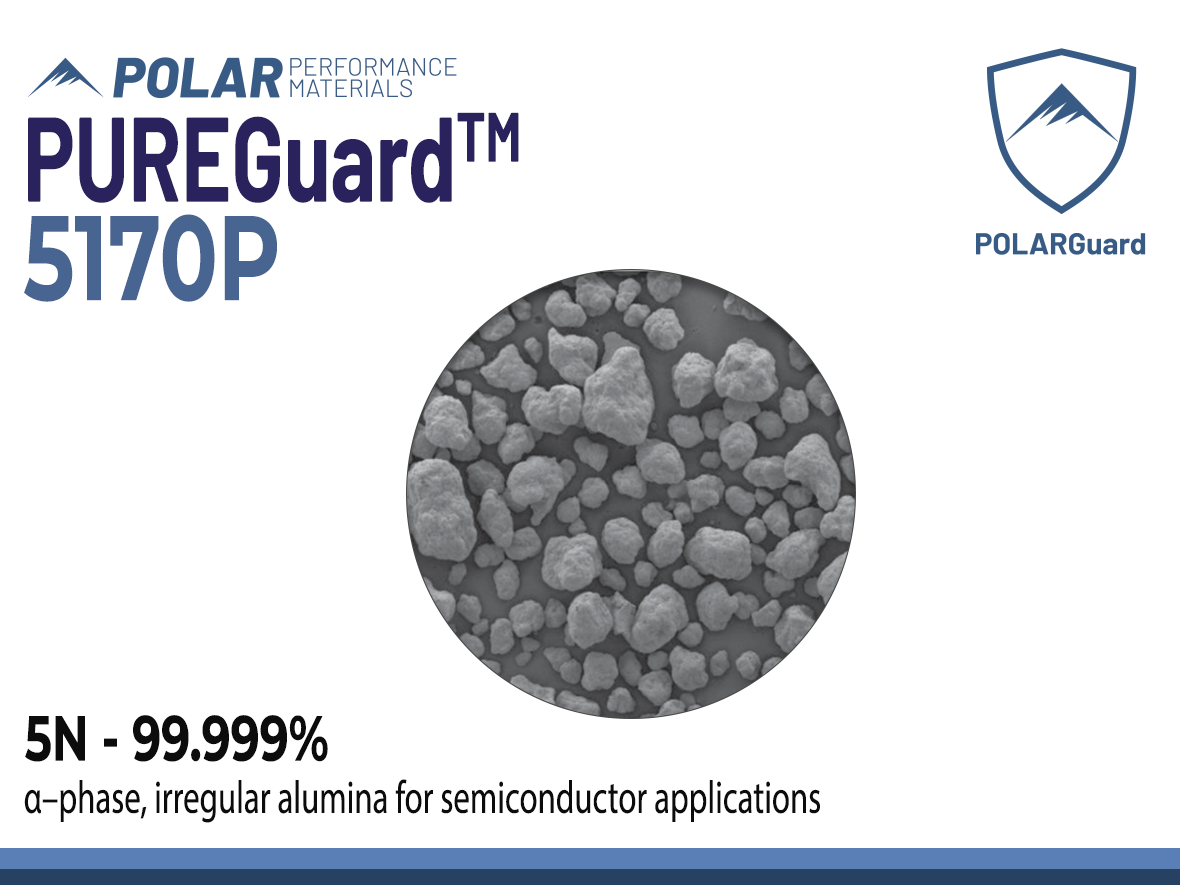
TECHGuard 5170P is a high-purity alumina product characterized by its 5N (99.999%) purity level. It features an irregular morphology and a surface area of 4-7 m²/g, optimized for semiconductor applications. This material offers uniform atomic-level coverage, making it suitable for a variety of high-reliability applications requiring excellent protection and high purity.
TECHGuard 5170P High Purity Alumina meets the following requirements:
- Manufactured using ISO 9001:2015 Certified processes.
- Ultra-low impurities
- Optimized Surface area
- Process stability
- High temperature resilience
- High quality in harsh conditions
Product Key Features
- Ultra High Purity — Ensuring consistent performance, reliability, and compatibility.
- Precise Particle Size Control — Engineered distribution for optimal packing density, flowability, and surface finish.
- Eco-efficient Manufacturing — Minimizing environmental impact while maximizing purity and quality.
Applications:
- Polar's PUREGuard line of products is engineered for a wider variety of applications, such as fillers for epoxy molding compounds, ceramic parts for semiconductor manufacturing, plasma etching, die handling, gold wire bonding, chemical mechanical polishing (CMP), etc.
Technical Specifications
| General Properties | |||||||||||
| Density (g) | 0.3-0.5 g/cm3 | ||||||||||
| Morphology | Irregular | ||||||||||
| Particle size (D50) | 1.4-2.0 um | ||||||||||
| Purity | 99.999 % | ||||||||||
| Surface Area | 4-7 m2/g | ||||||||||
| Other Properties | |||||||||||
|
|||||||||||
| Chemical Properties | |||||||||||
| Phase | α | ||||||||||
Additional Information
Frequently Asked Questions about PUREGuard
The PUREGuard line is specifically designed for applications where there is no margin for error. In semiconductor manufacturing, a single particle imperfection can reduce chip value by 70% or more. Especially as nodes shrink and tolerances tighten, materials must meet uncompromising standards of cleanliness and consistency.
What purity is available used in Semiconductor Applications?
Both 4N and 5N purity can be used in semiconductor manufacturing, depending on the application requirements.
What documentation is available for semiconductor validation?
Polar provides full quality assurance reports, including particle size data, elemental analysis, and batch traceability. This supports customer audits and material validation for regulated programs.
How is PUREGuard used as a coating?
High-purity alumina can be used in thermal barrier coatings and alumina ceramic coatings for high-temperature environments.
High-purity alumina can come in either spherical or irregular shapes. Spherical particles are smooth and uniform, offering excellent flow, easy dispersion, and consistent packing. Irregular particles are angular and jagged, providing better mechanical interlocking and abrasion. Spherical morphology is ideal for coatings or pastes, while irregular morphology is ideal for structural ceramics or abrasives.
Can I request a customized particle size?
Yes. Standard distributions and customized sizing is available, including submicron options, to align with your coating or forming process. Our team can match existing specs or develop a tailored grade with full documentation.
How is PUREGuard used in Chemical Mechanical Polishing (CMP)?
CMP combines chemical and mechanical methods to achieve a flat, smooth surface on semiconductor wafers, which is essential for depositing subsequent layers of material in multi-layered ICs. CMP Slurries are usually made of an abrasive, like PUREGuard HPA, water, and chemicals like oxidizing agents or acids, which assist in the breakdown of the wafer.
What format of HPA should I use for coating applications?
Powder formats are primarily tailored for coating feedstocks. These are designed for high flowability and predictable deposition, with purity levels up to 5N depending on the application.
| Purity | Key Element concentration (ppmw) | |||
| Na | Si | Ca | Fe | |
| 5N | 10 | 8 | 5 | 5 |
High Purity Alumina (HPA) in the Semiconductor Industry
The semiconductor industry demands materials of the highest quality and consistency, and High Purity Alumina (HPA) plays a critical role in ensuring the reliability and performance of cutting-edge technologies. With purity levels ranging from 4N (99.99%) to 5N (99.999%), HPA provides unparalleled advantages for semiconductor manufacturing processes and components.
Applications in the Semiconductor Industry
HPA can be used for a wide variety of applications, providing exceptional benefits. In the following table we tried to outline the applications the impact that HPA can have for Semiconductor related applications.
- Etching Components and Process Equipment
HPA is essential in the production of etch tool components used in advanced semiconductor manufacturing. Its high purity minimizes trace metal contamination, reducing defect rates in intricate devices such as integrated circuits (ICs) and microprocessors. - Ceramic Substrates and Wafer Handling
HPA is a key material for ceramic components like electrostatic chucks and insulating layers used in wafer handling. Its excellent dielectric properties and thermal stability ensure superior performance in high-temperature and high-frequency environments. - Protective Coatings for Semiconductor Tools
Alumina coatings derived from HPA improve the wear resistance and longevity of critical tools and components in semiconductor fabrication. The high hardness and corrosion resistance of HPA-based ceramics protect against chemical and mechanical degradation. - CMP Slurries for Polishing
Chemical Mechanical Planarization (CMP), a crucial process in semiconductor wafer fabrication, uses HPA as a base material for slurries. Its uniform particle size and exceptional purity ensure smooth, defect-free polishing, which is critical for creating high-performance devices. - Sapphire Substrates for LEDs and Optoelectronics
HPA is used to grow sapphire crystals for substrates in light-emitting diodes (LEDs) and optoelectronic components, which are integral to modern semiconductor applications. Sapphire's superior optical clarity and thermal conductivity are made possible by ultra-high purity HPA.
|
Application
|
Description
|
Impact on the Semiconductor Industry
|
|
Etching Components
|
Used in etching tool parts
|
Minimizes defect rates due to high purity, crucial for ICs and microprocessors.
|
|
Ceramic Substrates
|
Electrostatic chucks, insulators
|
Offers thermal stability and dielectric strength for high-temperature environments.
|
|
Protective Coatings
|
Enhances tool longevity
|
Improves resistance to wear and corrosion, extending equipment life.
|
|
CMP Slurries
|
Base material for polishing
|
Provides smooth, defect-free wafer surfaces essential for high-performance chips.
|
|
Sapphire Substrates
|
For LEDs and optoelectronics
|
Ensures optical clarity and thermal conductivity for efficient LED production.
|
Benefits of HPA in Semiconductor Manufacturing
- Reduced Contamination Risks
- Improved Dielectric Performance
- Thermal and Mechanical Stability
- Eco-Friendly Production
|
Property
|
Benefit
|
Description
|
|
Purity Level
|
4N (99.99%) to 5N (99.999%)
|
Reduces contamination, increases yield, and ensures device reliability.
|
|
Dielectric Performance
|
Excellent insulation properties
|
Allows for better performance in high-frequency applications.
|
|
Thermal Stability
|
Maintains integrity under heat stress
|
Critical for maintaining operational consistency in semiconductor processes.
|
|
Environmental Impact
|
More sustainable production
|
Aligns with industry trends towards eco-friendly manufacturing processes.
|