
Advanced Packaging
Flip Chip, Wafer level and 3D memories
- Home

- Semiconductors
- Advanced Packaging
- Fan-Out Packaging (FO-WLP & FO-PLP)
Fan-Out Packaging (FO-WLP & FO-PLP)
Fan-Out Packaging
Fan-Out Packaging, more commonly known as Fan Out Wafer-Level Packaging (FO-WLP), is an advanced integrated circuit packaging. Currently, it is only FO-WLP that is established but the increasing demand for higher throughput & limitations of FO-WLP pushed for the development of Fan-Out Panel-Level Packaging (FO-PLP).
To better understand FO-WLP Packaging, it is important to discuss the fundamentals of wafer-level packaging.
In rudimentary semiconductor packaging techniques, wafers, which are thin, circular discs of silicon with high crystallinity, are typically diced before they are packaged and encapsulated by an epoxy molding compound. This results in a device that is larger in size relative to the silicon die


The demand for smaller and more powerful devices led to the development of wafer-level packaging (WLP). In conventional WLP, the integrated circuit (IC) is fabricated on the wafer. The packaging components are attached onto the wafer before it is diced into packages that have the same size as the chip, rendering WLP as a true chip-scale package.
This has a caveat, however, and that is the limited number of external contacts that can be accommodated by conventional WLP packages. To address this, Fan-Out WLP was developed.
Fan-out refers to routing electrical connections beyond the size of the silicon chip. In FO-WLP packages, the chip is embedded in a molding material and redistribution layers (RDLs) create routing areas for external connections. RDLs are either formed through thin film deposition or photolithography.
In FO-WLP, the wafer is also diced first, but they are placed face-down & precisely repositioned onto a carrier to have space around the dies for fan-out connections. Precise position is crucial to yield quality RDLs later on.
A molding material is dispensed over the repositioned dies, creating a reconstituted wafer. This wafer is thinned out and cleaned, and the RDLs are formed. Fine copper lines reroute connections away from the die, allowing FO-WLP to have higher I/O count & better electrical and thermal performances.
Solder balls are deposited onto the RDLs to form external interconnects, which will connect the packages to the PCB. The wafer is then cut into individual packages, and additional testing is done to check its quality and integrability with other components in electronic devices.

The development of FO-WLP packages are getting more competitive to meet the ever increasing demand for more powerful and more compact electronic devices. It meets the demand for mid-range to high-end applications since it allows for >500 I/Os with less than 8um line/space.
It is reported that Apple iPhones use TSMC’s high density FO-WLP packages Currently, these are the leaders in the development & manufacturing of FO-WLP alongside the architecture they offer:
Table: List of Manufacturers & Their FO-WLP Packages (Modified from Semiconductor Engineering, 2018)
| Manufacturer | FO-WLP Package Type |
| TSMC | Integrated Fan-Out (InFo) |
| ASE | Embedded Wafer Level Ball Grid Array |
| Amkor Technology | Embedded Wafer Level Ball Grid Array Semi Wafer Integrated Fan-out Technology |
| Deca Technologies | M-Series |
| Huatian Technology | Embedded Silicon Fan-Out |
| Infineon | Embedded Wafer Level Ball Grid Array |
| JCAP | Embedded Chip Package |
| Nepes (originally developed by Freescale) | Redistributed Chip Package |
| SPIL | Thermoplastic Polyimide Fan-Out |
| STATS ChipPAC | Embedded Wafer Level Ball Grid Array |
FO-WLP is typically used and integrated into electronic systems for the following reasons:
- Miniaturization
- Improved Performance
- Better Efficiency
- Cost Efficiency
Miniaturization
Because FO-WLP has interconnects beyond the chip, more components can be integrated into smaller, single packages. The RDLs also allow for high-density interconnections with other dies such as CPU chips.
To put it in perspective, if a device will only use traditional semiconductor packages, the footprint & package height will be remarkably larger. Typical semiconductor packages approximately have a footprint that is 150~200% of the original die. FO-WLP is 30% thinner than traditional BGAs.
If a typical semiconductor package will be designed to yield comparative I/Os as FO-WLP, a much larger and thicker package is needed, which won’t meet the size requirements for smaller & powerful devices such as smartphones

Better Performance
FO-WLP also has shorter interconnects, maintaining signal integrity with reduced signal delays and electrical resistance.
Lower electrical resistance is ideal because this means more current is transported, increasing device speed. Shorter interconnects also have lower capacitance, which lessens the slowdown of electrons and minimizes the occurrence of crosstalk; the change in voltage in one interconnect affects the neighboring interconnect.Improved Efficiency
Likewise, the shorter interconnects mean shorter signal paths, reducing the risk of interference and better thermal management. A shorter signal path means that the distance heat travels to a cooler place is also shorter. It also makes the device have lower signal delays, lower power consumption, and a more even current distribution.

Cost Efficiency
The initial cost for fabricating fan-out packaging is steeper compared to other semiconductor packages because its complex manufacturing process requires an initial investment for new infastructure. However, in the context of package size, fan-out packaging can be the more cost-efficient option.
Fan-out packaging doesn’t require an interposer. It also doesn’t require traditional substrate, thus leading to a lower material cost and more straightforward yet complex manufacturing process with higher I/Os.
Cost efficiency is also the reason why manufacturers are trying to shift from FO-WLP to FO-PLP. Silicon wafers are circles with diameters ranging between 100mm to 450mm, while silicon panels are typically 510 x 515mm. By using panels, yield improves while cost is reduced.
Applications of FO-WLP & FO-PLP
Fan-out packaging is typically used in the following applications:
- Mobile and consumer electronics
- Automotive components
- High-performance computing
- Telecommunications
Mobile & Consumer Electronics
Fan-out packaging is most prominent in small devices such as smartphones and wearable technology because of its small size and improved performance. This packaging design is typically used in mobile devices’ central processing units (CPUs) & mobile application processors (APs).
Two key players within the mobile device industry are known to use FO-WLP— namely, Apple & Samsung. It is reported that Apple’s A20 chip is packaged by Taiwan Semiconductor Manufacturing Company (TSMC) using their InFo process.
On the other hand, Samsung’s Exynos 2400 packaged by Deca Technologies also uses FO-WLP, and they are currently developing Fan-Out Wafer-Level Package - Heat Path Block (FOWLP-HPB) for their mobile application processors.
Millimiter-Wave Applications
FO-WLP is used in automotive radar & telecommunications systems as part of the antenna-in-package solutions for radar sensors & RF modules. FO-WLP is capable of having on-package antenna integration, which is why it is typically the option for this application.
JCET is reported to use FO-WLP for their 4D Millimeter-wave Radar to meet L3+level autonomous driving requirements. They also featured that their radar packaging has a smaller formfactor with antenna on mold and double-sided RDL packaging.
High Performance Computing
The demand for high performance computing (HPC) is growing, which is mostly driven by artificial intelligence, big data analytics, and scientific research. HPC requires specialized chips because unlike the standard CPUs, they perform thousands of parallel computations.
Because of this growing demand, several key players are racing to increase the yield for their HPC chips. Two of which are Advanced Micro Devices & NVDIA, which are collaborating with TSMC & different OSAT providers to integrate FO-PLP in their next-generation AI GPUs and multi-die applications.
Design Challenges in Fan-Out Packaging
While Fan-out packaging sounds ideal on paper for smaller devices requiring better I/Os & integration, it also has its own share of design challenges brought by its more complex manufacturing processes:
- Wafer warpage & die shift
- Protrusion
- Board-level reliability

Wafer Warpage & Die Shift
Warpage refers to the deformation of the silicon wafer during fabrication likely due to the mismatch between the thermal expansion coefficients of the materials used as well as curing & process temperatures.
When different materials are exposed to varying temperatures, they expand and contract at different rates, inducing stress onto the wafer. There are two modes of wafer warpage: compression & tension. Recall that semiconductor packages are processed from a high temperature and then cooled down:
Compression
Occurs when the material used onto the silicon wafer has a larger CTE relative to silicon during cooling. As the temperature lowers, the film contracts more than the silicon wafer. Because the wafer limits the contraction of the film, a compressive stress is applied onto the film, which then warps the wafer into a concave shape.Tension
Happens when the material such as a film applied onto the wafer has a lower CTE relative to silicon during cooling. As the temperature lowers, the silicon wafer contracts more than the film, applying a tensile stress onto the material, making it expand more, which then warps the wafer into a convex shape.
Warpage can lead to die shift, compromising the quality of RDLs & the device’s electrical performance, and will lead to lower yield. Die shift refers to the unintentional displacement of the silicon die during the fabrication process, and as previously mentioned, in FO-WLP fabrication, die placement dictates the quality of the package.
Protrusion
Also called as die stand-off, protrusion results from the shrinkage of the molding material during the cure process. It can also be the result of warpage from CTE mismatch and variations in die thickness. Protrusion is the height difference between the top surface of the molding material or the RDLs in fan-out packaging, and will also affect the quality of the RDLs.
Outside of CTE mismatch, Protrusion happens when the non-uniform curing of the molding material pulls the die, displacing it vertically. Variation in die thickness can also lead to protrusion; a thicker die will have parts of it sticking up in the molding material surface while a thinner die may be underexposed or placed lower relative to the molding material plane.
Board-Level Reliability
Because FO-WLP is a wafer-level package, it shares similar challenges with other WLPs, namely, stress management of the silicon chips and the solder joints. The lack of substrate means that there is no buffer layer between the die and the printed circuit board, introducing added thermal stress onto the package & areas where stress is concentrated.
The lack of the substrate also means that FO-WLP has less structural support, making it more sensitive to mechanical stress such as shock from dropping and induced stress from the circuit board flexing. There have been several measures done to optimize board-level reliability, including controlling fabrication parameters, improving material properties, and strategically designing package architecture.
CAPLINQ Solutions for Fan-Out Packages
CAPLINQ offers encapsulation solutions for both fan-in and fan-out as well as wafer-level & panel-level packaging. Our line of products focuses on having low-warpage and high reliability for thin package applications.

Henkel LOCTITE ABLESTIK BSP 125 is a black hybrid film designed for WLCSP back side laser marking and chip protection applications. It meets the technical requirements for WLP backside protection, specifically reworkable after lamination, high reliability, low outgassing, consistent bondline thickness, and low-warpage.
BSP 125 protects silicon dies from chipping and cracking, warpage, and package damage during the SMT placement process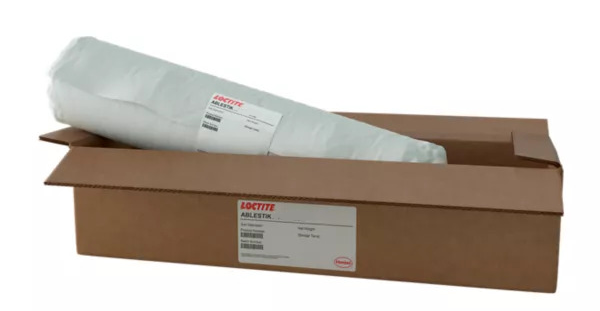
Frequently Asked Questions About Fan-Out Packaging
What’s the difference between FO-WLP, 2.5D, and 3D packaging?
FO-WLP is the cheapest package among three and the biggest difference it has between the two other packages is that it doesn’t use any interposer or vias. 2.5D packaging has an interposer & 3D packaging has Through-Silicon Vias (TSVs). FO-WLP only has a single layer package built around dies while 2.5D packaging has dies side-by-side on the interposer. 3D packaging has dies stacked vertically.
What is the main advantage of using RDLs in FO-WLP?
The RDLs, made with photolithography, enable fine-pitch routing with small line widths and spaces. This improves electrical performance by lowering resistance and inductance. It also allows for a higher density of connections than traditional package substrates.