Electronic Device Substrates
The Core of Semiconductor Technology
- Home

- Electronics Assembly
- Substrates
- EMI Absorbers and Magnetic Shielding Materials
EMI Absorbers and Magnetic Shielding Materials
Electromagnetic interference (EMI) occurs when unwanted electromagnetic energy generated by an electronic system disrupts the operation of another system or circuit. During operation, voltages and currents within electronic circuits generate electric and magnetic fields around conductors, which together form an electromagnetic field.
Static or slowly varying fields typically do not cause interference. EMI becomes significant when electrical signals change rapidly, such as in switching power supplies, high-speed digital electronics, and RF systems. These fast changes produce time-varying fields that can propagate as electromagnetic waves and carry unwanted electromagnetic energy.
This energy can couple into nearby circuits through cables, connectors, and enclosures, or through the air, leading to conducted EMI, radiated EMI, and near-field coupling. These effects are common causes of signal noise, data errors, and electromagnetic compatibility (EMC) issues in electronic devices.
EMI Sources and Coupling Paths in Electronic Assemblies
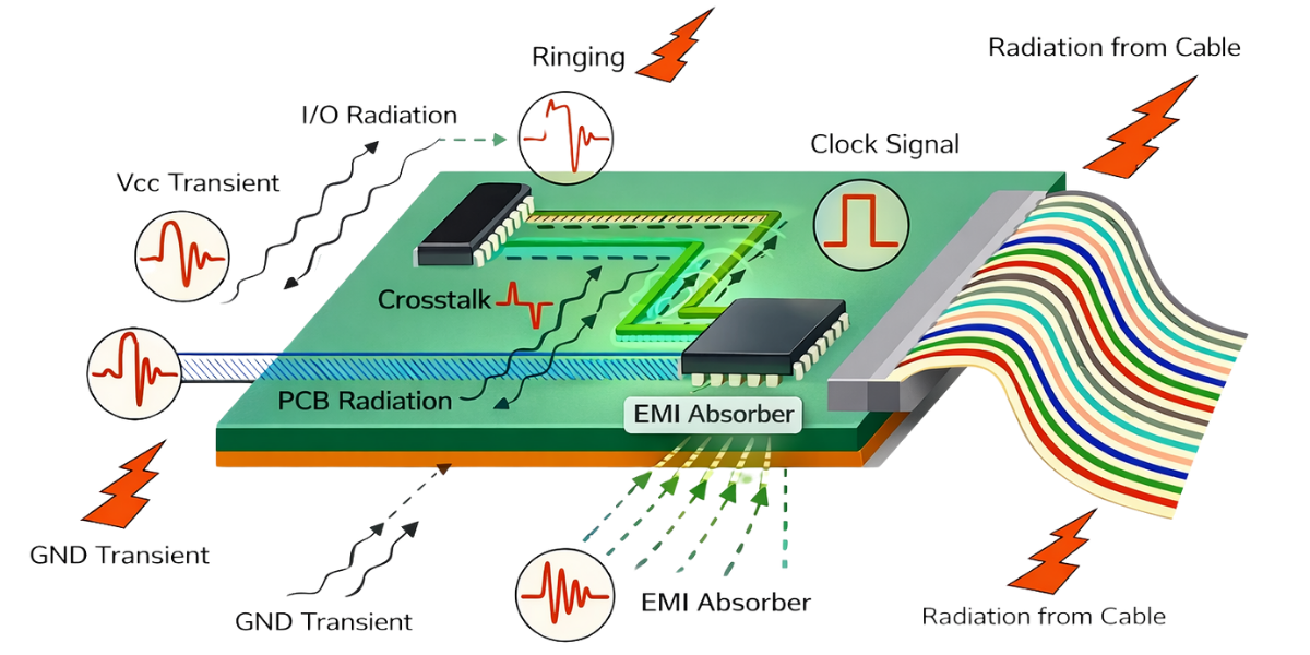
Common sources and propagation paths of EMI in electronic assemblies
- Near-source noise generation: Fast-switching components such as power converters, clock lines, and high-speed digital signals generate high-frequency electromagnetic noise directly at the source.
- Coupling within the PCB: Poor layout choices, including long traces, split ground planes, and inadequate return paths, allow noise to couple into adjacent signal and power paths through crosstalk and ground bounce.
- Radiation from the PCB: Once coupled, high-frequency noise can radiate directly from PCB traces and planes, acting as unintended antennas.
- Emission through cables and connectors: Noise reaching I/O and cable interfaces can radiate efficiently into the surrounding environment, becoming a dominant source of EMI.
EMI can cause multiple issues in electronics, including:
Device Malfunction
EMI can cause electronic devices to behave unpredictably or stop working temporarily.
Signal Distortion
Electromagnetic interference can corrupt or weaken signals in communication systems.
Circuit Overload
Strong EMI can introduce extra current or voltage into circuits, potentially damaging components.
Safety Hazards
EMI can disrupt critical systems, creating dangerous situations.
As electronic devices have become faster and more compact, the risk of electromagnetic interference (EMI) disrupting their operation has increased. EMI absorbers were developed to control unwanted electromagnetic energy, helping reduce noise and protect sensitive circuits in high-performance electronics.
Anatomy of an EMI Absorber
EMI absorbers are engineered materials used to reduce electromagnetic interference in electronic devices and assemblies. They absorb unwanted electromagnetic energy and convert it into heat, helping prevent signal degradation, noise coupling, and performance issues in high-speed and high-frequency electronics.
EMI absorbers are typically supplied as thin, flexible sheets that contain specialized magnetic particles which absorb EMI without introducing electrical conductivity. They can be ordered with or without a non-conductive pressure-sensitive adhesive (PSA).
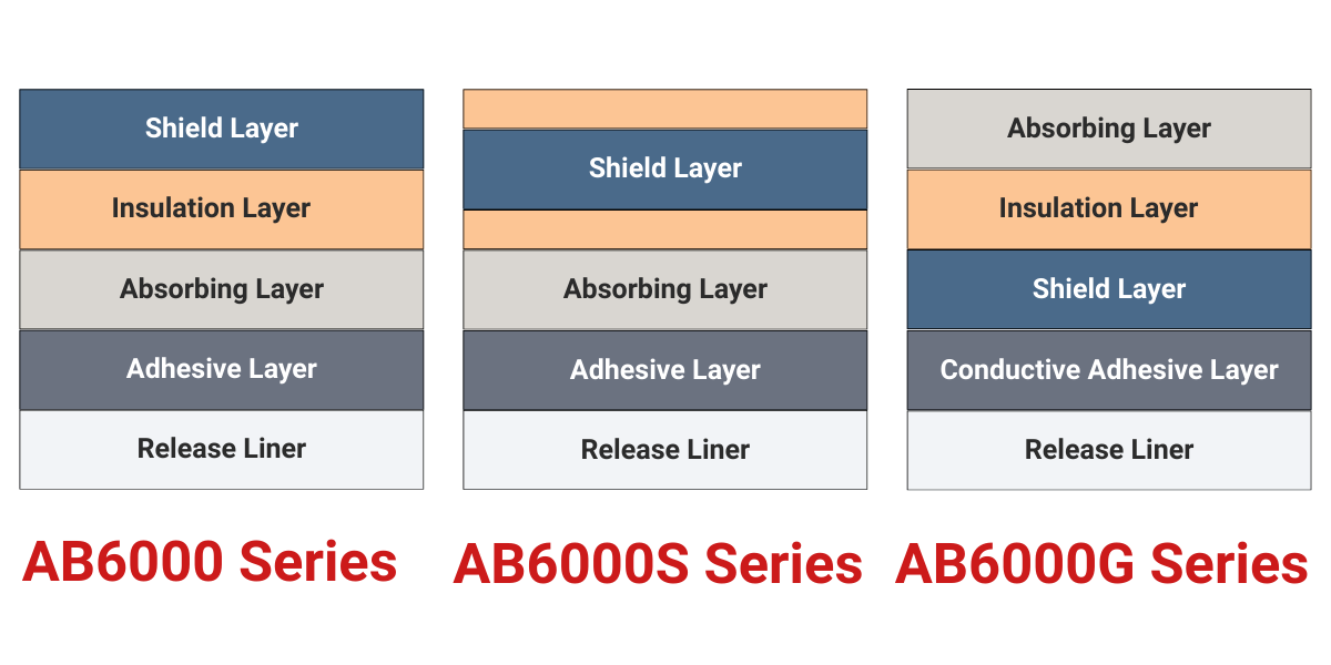
Shield Layer — Blocks or reflects incoming electromagnetic waves to provide the primary EMI protection.
Insulation Layer (optional) —Prevents electrical shorts while maintaining EMI control between conductive layers.
Absorbing Layer — Converts electromagnetic energy into heat, reducing reflections and lowering interference.
Adhesive Layer (optional) — Allows easy and secure attachment of the absorber to devices or enclosures.
Release Liner (optional) — A removable layer that protects the adhesive until the absorber is ready to be applied.
EMI absorbers can be applied in multiple ways to reduce EMI in electronic devices and assemblies, including placement at noise sources, on enclosure surfaces, between module components, and on cables.
Directly to the noise source
Minimizes EMI at its origin by absorbing emissions from traces, ICs, and processors
Attach directly to and/or opposite side of noise source (traces, cameras, digital IC's, chip, microprocessor)
Enclosure Surfaces
Reduces internal reflections and re-radiation within the housing
Between Module Components
Helps suppress coupling between adjacent components
Cables
Attenuates radiated noise along round or flex cables
Where EMI Absorbers Deliver the Most Value
EMI Absorbers have become an essential solution for electronic systems that demand high signal integrity, low noise, and reliable performance as operating frequencies continue to increase.
They provide an effective balance between traditional shielding approaches and more complex mitigation techniques by absorbing and dissipating unwanted electromagnetic energy rather than reflecting it back into the system. This helps suppress radiated and conducted EMI, reduce crosstalk, and stabilize sensitive circuits without introducing additional interference paths.
By controlling electromagnetic noise at its source, EMI absorbers enable designers to improve system reliability and performance while avoiding the size, weight, and design constraints often associated with conventional metal shielding or over-engineered EMI solutions.

Primary driver: Safety, reliability, and system performance.
Reduction of EMI that interferes with ADAS and vehicle communication systems.
Protection of sensitive electronics from generated noise.
Stable performance across wide temperature ranges and harsh automotive environments.
Primary driver: User experience, performance, and reliability.
EMI Absorbers enable:
- Reduction of EMI that affects wireless signals.
- Protection of compact, high-speed electronics from internal electromagnetic noise.
- Consistent high quality performance.
Primary driver: Patient safety, signal integrity, and device reliability.
EMI Absorbers allow:
- Suppression of radiated and conducted EMI that can interfere with imaging systems and life support electronics.
- Protection of sensitive electronics from external EMI and internal noise.
- Stable electrical and thermal performance to ensure accurate diagnostics and reliable operation.

Primary driver:
Signal integrity, reliability, and mission safety.
EMI Absorbers enable:
- Suppression of radiated and conducted EMI that can disrupt radar, avionics, and communication systems.
- Protection of sensitive electronics from high-power RF, lightning strikes, and electromagnetic pulses (EMP).
- Stable thermal behavior in extreme operating environments.
Key Features of EMI Absorbers
Excellent grounding with small contact areas, helping enable micro-electronic design.
Low electrical resistance/high adhesion helps provide reliable EMI shielding and grounding for a wide range of frequencies.
High performance on a variety of substrates for design versatility.
Can reduce the need to use a primer when bonding some LSE (Low Surface Energy) substrates.
Long-term performance at high temperatures (105ºC) for demanding applications.
High-performance in humid conditions for greater design flexibility.
CAPLINQ Solutions for Electromagnetic Interference Management
As electronic systems continue to increase in speed, density, and power, controlling electromagnetic interference (EMI) becomes a critical challenge. Without effective EMI management, unwanted electromagnetic energy can degrade signal integrity, reduce reliability, and compromise system performance.
EMI Solutions with 3M EMI Absorbers
Electromagnetic interference (EMI) management focuses on controlling unwanted electromagnetic energy, reducing noise, and protecting sensitive electronics from interference. The EMI absorber solutions below are commonly used in a variety of electronic systems and applications.
AB7000E Series
The 3M AB7000E Series EMI Absorber is a flexible polymer sheet loaded with soft metal flakes, designed for near-field EMI suppression from 300 MHz to 4 GHz, with optimal performance between 800 MHz and 2.5 GHz. It features a non-conductive acrylic pressure-sensitive adhesive for easy application (also available without adhesive) and is ideal for absorbing EMI inside and around electronic devices and assemblies.
AB8000 Series
3M EMI Absorber AB8000 Series is a high-temperature magnetic near-field EMI absorber material for electronic applications from
300 MHz to 4 GHz. The composite material features a silicone carrier resin for stable solder reflow and strong attachment to FPCs ,
along with magnetic fillers to suppress near-field EMI noise inside and around electronic devices and assemblies.
EM25TP Series
The 3M EM25TP Flux Field Directional Material is a magnetic composite with a carrier resin and magnetic fillers, designed for EMI absorption and magnetic shielding. It offers high permeability and magnetic loss to suppress EMI noise in its target frequency range (up to 15 MHz) and can prevent short circuits in electrical systems. With options like acrylic PSA for easy application and a black PET top film for durability, it’s ideal for custom high-performance stackups that efficiently couple and redirect magnetic fields.
AB60005SHF Series
The 3M AB6000HF/SHF Series is a hybrid EMI absorber combining a metal shielding layer and an absorbing layer separated by insulation. It provides high-frequency EMI shielding and noise suppression (up to 18 GHz) for improved signal-to-noise ratio, and features a pressure-sensitive acrylic adhesive with a removable liner for easy application. Available in sheets and rolls, it’s ideal for complex EMI control applications.
Why EMI Absorbers are Strong Candidates for High-Performance Electronic Systems
Among available EMI control solutions, hybrid and magnetic absorbers provide a practical balance between shielding effectiveness and design flexibility. They combine high-frequency absorption, magnetic field suppression, and predictable performance across varied geometries, while remaining compatible with complex assemblies and sensitive components.
In modern electronic systems, where high-speed circuits, dense layouts, and mixed-signal components can create localized EMI hotspots, these absorbers offer a way to maintain signal integrity, reduce noise, and protect sensitive electronics without compromising assembly design or reliability.
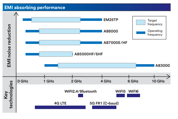
| 3M EMI Absorber Series | Frequency Range | Description |
|---|---|---|
| AB6000HF / SF Series | <18 GHz | Hybrid absorber for high-frequency EMI; combines metal shielding and absorbing layers; sheets and rolls; easy application with PSA |
| EM25TP Series | <15 MHz | Magnetic composite for EMI absorption and magnetic shielding; high permeability and magnetic loss; suitable for custom stackups; optional PSA and PET top film. |
| AB7000E Series | 300 MHz - 4 GHz (Optimal 800MHz - 2.5 GHz) | Flexible polymer with soft metal flakes; ideal for near-field EMI suppression; available with or without acrylic PSA. |
| AB8000 Series | 300 MHz - 4 GHz | High‑temperature magnetic near‑field absorber with silicone resin and magnetic fillers. |
For complex, high-speed electronic systems where EMI suppression, field uniformity, component sensitivity, and long-term reliability must all be balanced, hybrid and magnetic EMI absorbers provide a predictable and manufacturable solution that meets both performance targets and design constraints.
AB7000E SERIES
3M EMI Absorber AB7000E Series is an EMI suppression absorber for near-field applications from 300 MHz to 4 GHz Target
frequency range – or the optimal range for peak performance – is 800 MHz - 2.5 GHz. Consisting of a flexible polymer resin loaded
with a filler of soft metal flakes, this sheet is excellent for EMI absorption at frequencies from 300 MHz to 4 GHz.
An acrylic non-conductive, pressure-sensitive adhesive on one side makes application fast and easy, though this EMI absorber sheet is also available without adhesive. These sheet-type 3M EMI absorbers are great for absorbing near-field EMI inside and around electronic devices
and assemblies.
Key Features
- High permeability
- Broad operating frequency range from 300 MHz to 4 GHz
- Long shelf life (18 months)
- Broader temperature performance than AB7000HF Series
- Available with and without adhesive
- Multiple thicknesses available
- Release liner for easy handling
- Acrylic pressure sensitive adhesive
- Halogen free
Available Versions
- AB7050E-WO — 0.55mm thickness, 210 mm X 297 mm, without adhesive
- AB7020E-WO — 0.25 mm thickness, 210mm X 297 mm, without adhesive
- AB7010E-WO — 0.13mm thickness, 210mm X 297 mm, without adhesive
Controlling EMI with 3M Electrically Conductive Double-Sided Tape 5113DFT
3M Electrically Conductive Double-Sided Tape 5113DFT is an electrically conductive double-sided fabric tape (DFT) that provides
high adhesion, low electrical resistance, long shelf life, resistance to high temperature and humidity and excellent grounding and
shielding performance. It features a proprietary polyolefin XYZ-axis conductive pressure sensitive adhesive (CPSA) and a conductive
matrix carrier (a nickel/copper/nickel-coated conductive woven carrier).
This grounding tape provides excellent adhesion to a variety of substrates including metals and plastics and helps control signal
interference through passive intermodulation (PIM) mitigation for higher signal integrity and performance.
The following are the key features of 3M Electrically Conductive Double-Sided Tape 5113DFT:
Excellent EMI Shielding in Bond Line Gap
The material maintains strong EMI shielding effectiveness even within thin or uneven bond line gaps. This ensures continuous electromagnetic protection where traditional shields or gaskets may be less effective.
Excellent grounding with small contact areas for microelectronics
The material enables reliable electrical grounding even when contact areas are very small, as is common in miniaturized electronic designs. This makes it well suited for high-density microelectronics where space and contact geometry are limited.
Isotropic XYZ-axis conductivity through the adhesive
The adhesive provides uniform electrical conductivity in all directions, ensuring reliable grounding and consistent electrical performance across complex assemblies. This helps prevent signal discontinuities and improves overall EMI control.
Long-term performance at high temperatures (105 ˚C)
The material is designed to maintain stable electrical and mechanical performance during prolonged exposure to elevated temperatures. This ensures reliable EMI control and grounding in applications where thermal stress is a concern.
Frequently Asked Questions About EMI Absorbers
What if I need a thicker absorber than what you offer?
EMI Absorbers can be customized as needed, reach out to us.
Can EMI Absorbers be customised (ex. Higher frequency, different electromagnetic property, UL flame rating)?
Yes, EMI Absorbers can be customized as needed.
Suppress electromagnetic interference and improve signal integrity in advanced electronic systems.
Talk to our engineers about selecting the right materials for your package architecture, thermal budget, and long-term reliability requirements.