
Advanced Packaging
Flip Chip, Wafer level and 3D memories
- Home

- Semiconductors
- Advanced Packaging
- Package On Package (PoP)
Package On Package (PoP)
Package on a Package (or Package on Package, PoP) is an integrated circuit packaging that vertically stacks two or more packages (typically discrete or memory semiconductors) to ball grid arrays, which are soldered onto printed circuit boards.
What is Package on Package?
PoP was designed in response to the growing need for miniaturization of semiconductor devices as electronic devices become smaller and thinner. Typically, PoP has two configurations:
Mixed logic-memory stacking
This configuration is the most common one. The bottom package can be a processor, application-specific IC, or a microcontroller, which is soldered onto the board. On top of the bottom layer is a memory package (SRAM, DRAM, or flash memory) that is connected through interposers, pastes, or adhesive films.
Memory stacking
This configuration is less common. Essentially, the bottom layer is another memory device, and on top is another memory device. Likewise, the upper layer is connected to the bottom memory device either through an interposer, paste, or adhesive film.
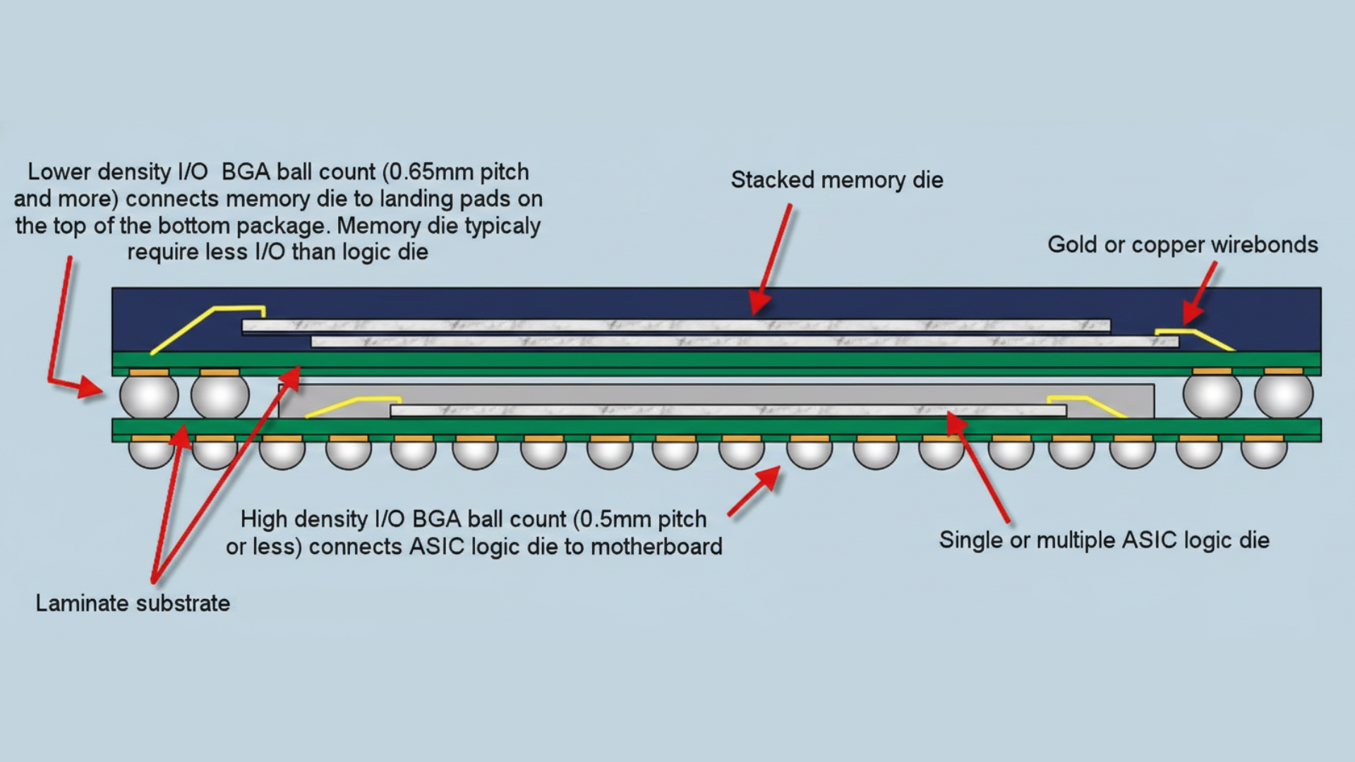
Typical vertical stacking architecture of PoP devices.
Key Features of PoP
PoP allows memory devices to exist within the same space as other packages without the need for more PCB space.
Less space between devices reduces resistance and signal delays, improving data transmission speed.
Shorter distances lead to lower power loss, improving battery usage in electronic devices such as phones.
PoP assembly integrates well with existing surface mount technology (SMT) assembly processes.
PoP Manufacturing Process
🔔 Reminder: Click each step below to expand and view its full description.
Sourcing PoP-Compatible Devices
In this step, the top surface of the bottom package must have a landing pad with patterns that match the solder ball grid of the top package. In this step, the coefficients of thermal expansions of the devices that will be stacked together should match (or relatively close to each other) to minimize warpage.
Solder Paste Application
Standard SMT process of applying solder paste onto the PCB is followed. For PoP assembly, solder pastes that can handle fine pitch, are tacky/viscous, and have no-clean formulation are generally recommended.
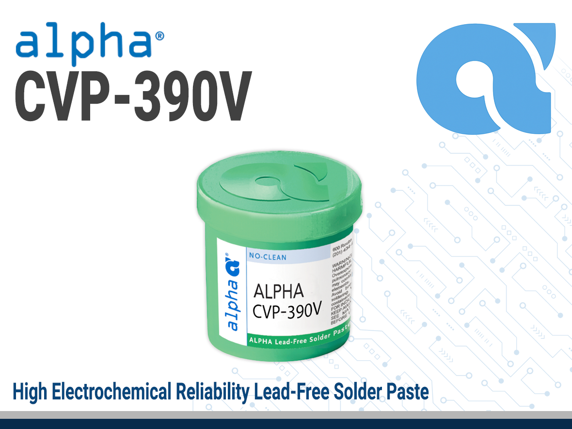
ALPHA CVP-390V Solder Paste
Zero-halogen, no-clean solder paste designed for fine-feature printing, high-reliability, and superior performance against HiP and NWO defects. Exhibits >2.00CpK for transfer efficiencies.
Base Package Mounting
A high-speed pick-and-place machine picks the Logic/SoC chip and places it onto the wet solder paste on the PCB.
Top Package Fluxing/Dipping
A different pick-and-place head picks up the top package and dips the solder balls into a thin film of PoP-specific flux or solder paste, which will ensure that the balls have enough tackiness to stick onto the landing pads of the bottom package.
Top Package Mounting
The fluxed Memory package is placed directly onto the "landing pads" on top of the bottom chip.
Reflow Soldering
The stack goes through the oven once in a “single pass.” As the solder liquefies and solidifies again, the flux must be tacky enough to keep the top package in place. Single pass reflow is typically advised for PoP assembly to minimize warpage and maximize production efficiency (i.e., the assembly spends less time in the oven).
Underfill Dispensing & Curing
Capillary action between the chips draws in the underfill, which are dispensed at the edge of the packages. For PoP assemblies, an underfill that effectively reinforces solder joints, minimizes thermal fatigue, and improves reliabilit in dense packages is recommended.
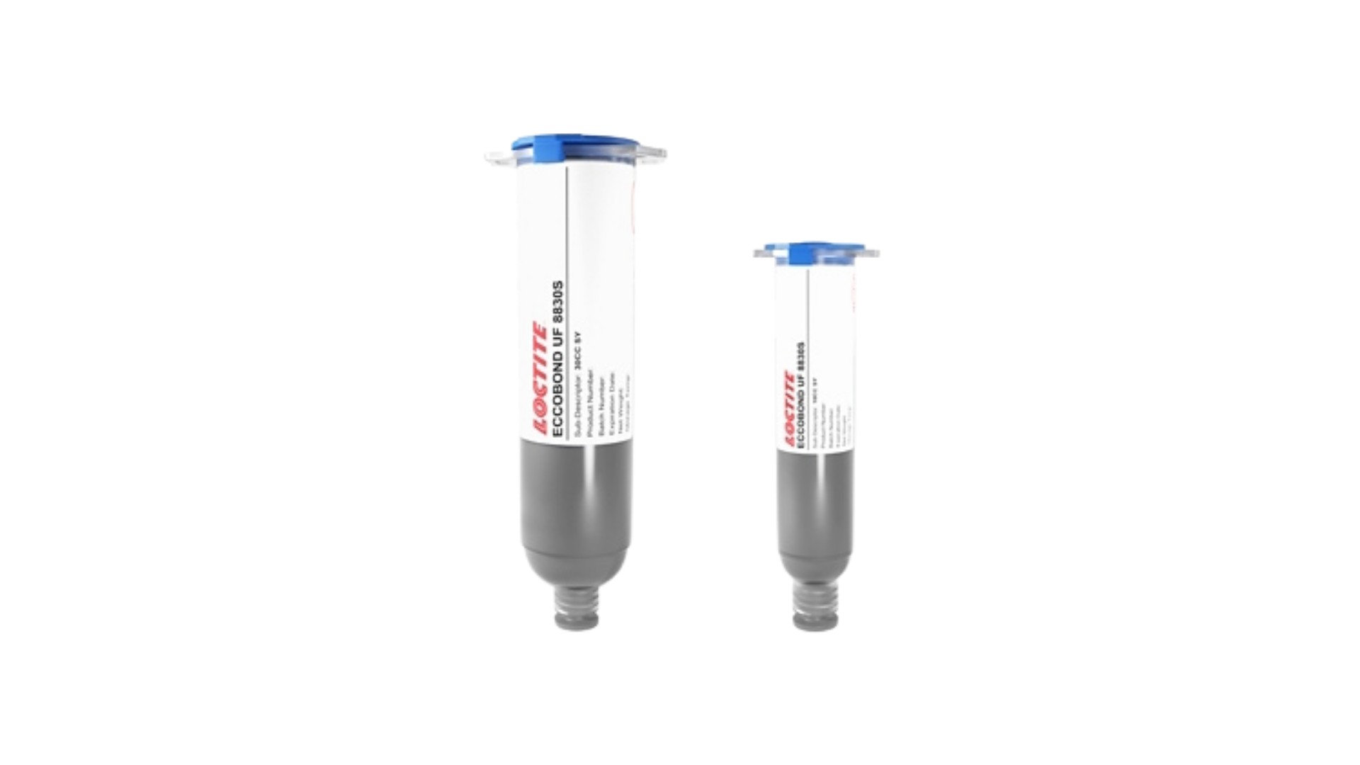
LOCTITE ECCOBOND UF8830S
Liquid epoxy capillary underfill for flip chip BGA applications. Achieves MSL L3/L2A and passes automotive reliability requirements after 4000 cycles without fillet cracks.
Quality Testing
X-ray inspection is used to verify that no "Head-in-Pillow" (HiP) or bridging occurred during the single reflow pass. HiP is a defect where the solder ball and the solder paste touch but fail to coalesce into a single, solid joint.
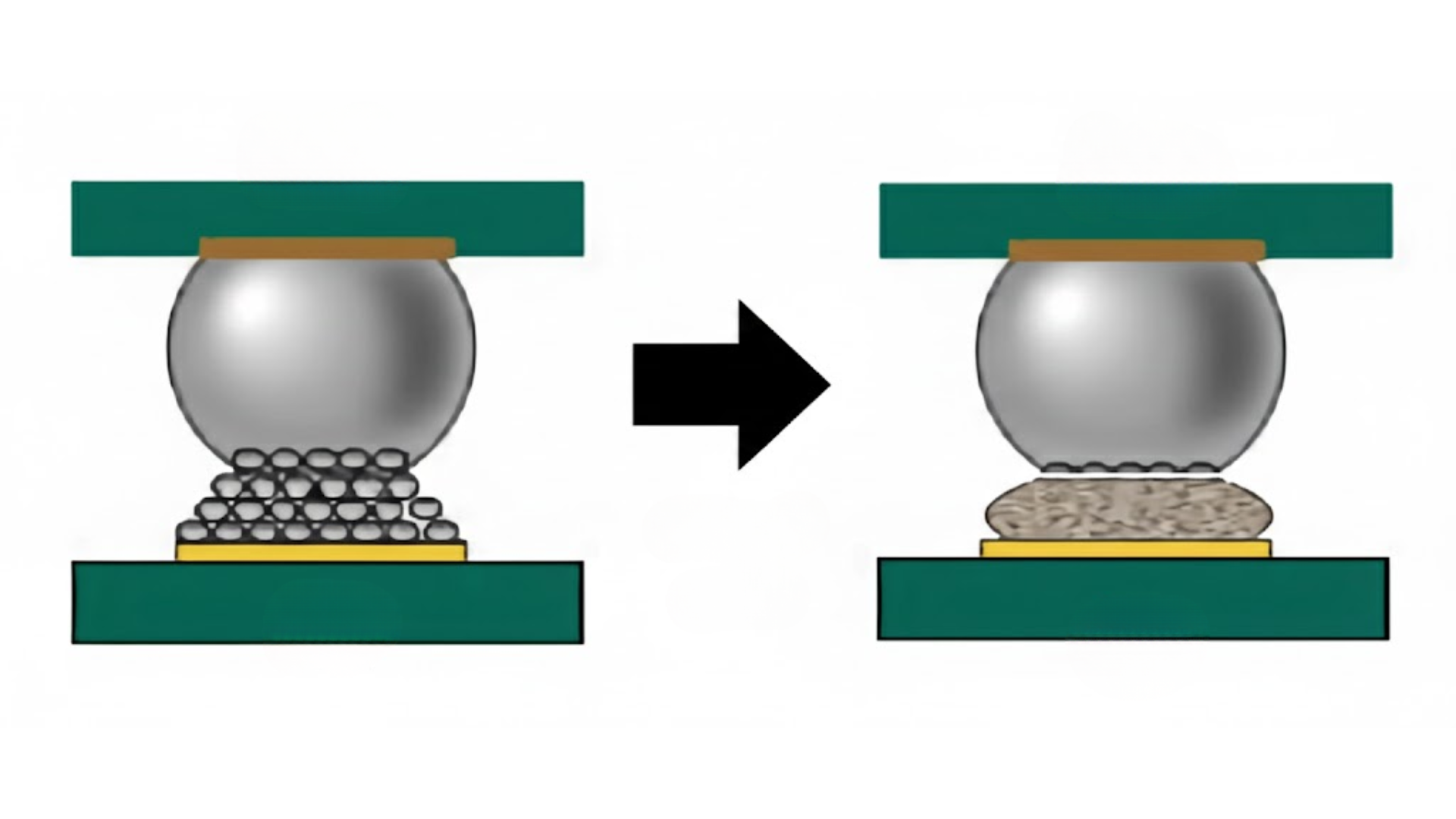
Figure. Visualization of HiP Defect
Coating
If the PCB with the PoP assembly is for a device that is exposed to harsh environments, a conformal coating is applied onto it. The conformal coating used must have thicknesses between 25 µm to 100 µmm and not prone to wicking or capillary flow, which eventually introduces thermal stress onto the solder joints between the top and bottom chip. We offer a broad range of conformal coatings for your PCB needs. HumiSeal’s sharp edge coverage (SEC) line of conformal coatings is formulated for PCBs with high density packages. SEC coatings solve issues on inadequate coating coverage on component corners and vertical edges, which can lead to failures from condensation or water immersion.
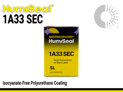
HumiSeal 1A33 SEC
Isocyanate-free polyurethane coating optimized for sharp edge coverage on high density packages. Engineered for rugged protection and UV traceability for inspection.
Design Challenges in PoP
Thermo-Mechanical Stress
Every material in the PoP stack (silicon, epoxy mold compound, organic substrate, and solder) has a different Coefficient of Thermal Expansion (CTE). When the device powers on, they expand at different rates. After hundreds of power cycles, this stress leads to solder fatigue. Micro-cracks form in the solder balls, eventually leading to a complete electrical "open."
Cooling and Heat Dissipation
PoP is a "thermal sandwich." The top package acts as an insulator for the bottom package. The bottom chip is usually the "hot" component, but it has no direct path to the surface to vent heat. Thermal Interface Materials (TIM) between the two packages or design "Thermal Vias" (copper chimneys) in the PCB to pull heat downward into the PCB are used.
To address the thermal and height limitations of standard PoP, the industry moved toward Fan-Out Wafer-Level Packaging (FOWLP) and specifically the Integrated Fan-Out (InFO) package.
CAPLINQ Solutions for PoP Assemblies
Frequently Asked Questions about PoP
What is the difference between PoP and SiP?
PoP (Package-on-Package) vertically stacks two finished, individually encased chips during the final PCB assembly to allow for supply chain flexibility and high memory bandwidth. SiP (System-in-Package) integrates multiple "naked" silicon dies and components into a single, specialized protective housing before it ever reaches the assembly line.
What is the difference between PoP and 2.5D packaging?
PoP (Package-on-Package) stacks two fully encased components directly on top of each other using traditional solder balls, whereas 2.5D Packaging places multiple naked dies (like a GPU and High-Bandwidth Memory) side-by-side on a middle layer called a silicon interposer.
Optimize your PoP Assembly Performance
Talk to our engineers about selecting high-reliability underfills, pastes, and coatings.