Advanced Packaging
Flip Chip, Wafer level and 3D memories
- Home

- Semiconductors
- Advanced Packaging
- 2.5D Packaging
2.5D Packaging
To understand what 2.5D packaging is, it is helpful to look at the evolution of semiconductor packaging, starting from conventional 2D approaches and progressing toward more advanced architectures.
Integrated circuit (IC) packaging is the process of enclosing a semiconductor die in a protective structure that provides mechanical support, environmental protection, and reliable electrical and thermal performance. A well-designed package protects the die from moisture and contaminants, manages heat dissipation, and enables electrical interconnection through bond wires, solder bumps, or lead frames. For encapsulation, epoxy molding compounds (EMCs) and liquid encapsulants are among the most widely used materials, with the choice depending on the specific package design and application.
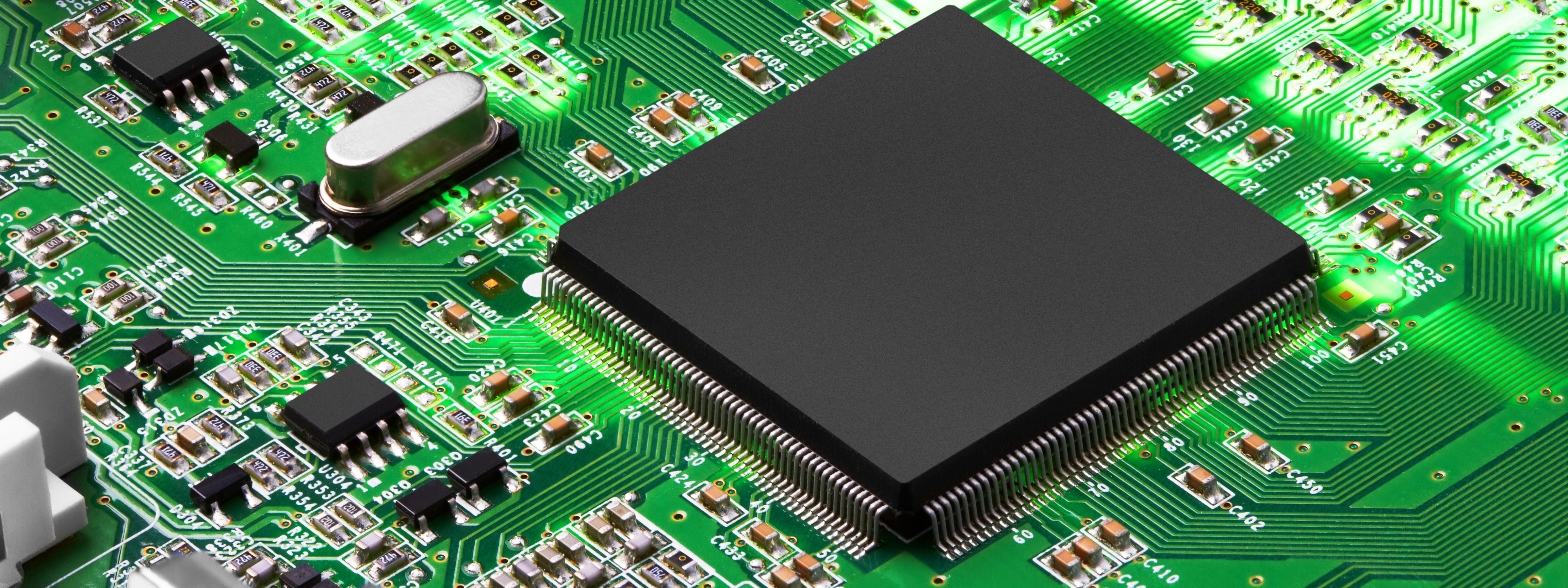
2D packaging represents the traditional form of IC packaging, where one or more chips are mounted side-by-side on a single plane. Electrical interconnection is typically achieved through wire bonding or flip-chip technologies, often in formats such as quad flat packages (QFPs), ball grid arrays (BGAs), or flip-chip BGAs (FCBGAs). These approaches have been used and refined over several decades and remain widely adopted due to their maturity, reliability, and cost-effectiveness.
Despite its maturity and widespread use, 2D packaging has several fundamental limitations that become critical as performance and integration requirements increase:
Limited Routing Density
In 2D packaging, all interconnects are routed on a single plane. As chips become smaller and more powerful, the number of required connections increases, but the available routing area does not scale accordingly. This leads to routing congestion and constrains electrical design flexibility.
Decreased Signal Integrity
Longer interconnect lengths and denser routing reduce signal-to-noise ratio and increase susceptibility to crosstalk and interference. This can degrade signal quality, increase latency, and limit achievable data rates in high-speed applications.
Power & Thermal Constraints
Increasing power density in advanced devices leads to higher heat generation. In conventional 2D packages, thermal paths are limited, making heat removal more difficult and potentially affecting reliability and long-term device stability.
Cost & Size Limitations
Adding functionality in 2D packages often requires larger substrates and more complex routing layers, which increases package size, material usage, and manufacturing cost, limiting scalability for highly integrated systems.
As the demand for higher performance and more highly integrated ICs increased, 2.5D packaging emerged as a response to the design limitations of traditional 2D architectures.
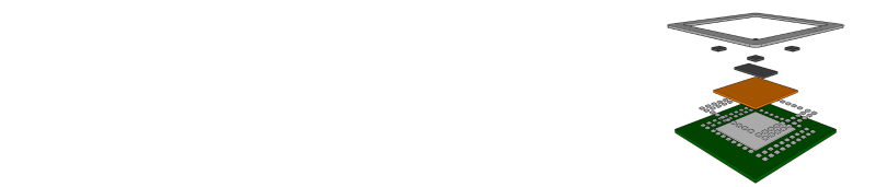
Anatomy of a 2.5D Package
2.5D IC packaging is an advanced semiconductor packaging technology in which multiple dies are placed side-by-side on a high-density silicon interposer. The interposer sits between the dies and the package substrate and contains dense wiring layers that electrically connect the dies to each other and to the external package I/O. This architecture enables heterogeneous integration of logic, memory, and accelerator dies within a single package, without vertically stacking them as in true 3D packaging.
.png)
Dies — Individual semiconductor chips with different functions, such as logic processors and high-bandwidth memory (HBM), placed horizontally on the interposer.
Silicon Interposer — The silicon bridge providing high-density wiring and fast electrical connections between dies and to the substrate.
Through-Silicon Vias (TSVs) — Vertical electrical connections through the interposer enabling high-bandwidth links between its top and bottom surfaces.
Microbumps — Fine-pitch solder bumps (typically <20 µm) that enable high-density die-to-interposer interconnects.
C4 Solder Bumps — Controlled Collapse Chip Connection bumps used to connect the interposer to the substrate where extreme density is not required.
Substrate — Provides the final electrical connection to the printed circuit board (PCB) and contains additional routing layers.
Underfill — A polymer material that improves mechanical stability, protects solder joints, and enhances long-term reliability.
Heat Sink / Lid — A thermal solution placed on top of the dies to dissipate heat and maintain safe operating temperatures.
In contrast to traditional 2D architectures, 2.5D packaging offers several structural and performance advantages that enable higher integration, better electrical performance, and improved efficiency:
Integration Flexibility
The use of a silicon interposer enables both homogeneous and heterogeneous integration, allowing chips with similar or different functions—such as logic, memory, and accelerators—to be combined within a single package.
High Routing Density
The silicon interposer provides fine-pitch, high-density routing, enabling multiple dies to be placed side by side with short, direct interconnects that would not be feasible on conventional organic substrates.
High I/O Density & Signal Integrity
Shorter interconnect distances reduce parasitics, improve signal-to-noise ratio, and enable higher input/output bandwidth with lower crosstalk and latency compared to traditional 2D packages.
Improved Power Efficiency
Reduced interconnect lengths minimize resistive losses and heat generation, while lower voltage requirements further reduce overall power consumption and improve energy efficiency.
Where 2.5D Packages Deliver the Most Value
2.5D IC packaging has become the dominant advanced semiconductor packaging solution for applications that demand extremely high bandwidth, heterogeneous integration, manageable thermal behavior, and production-scale reliability.
It occupies a practical middle ground between conventional 2D package architectures and true 3D logic stacking, delivering most of the performance and integration benefits enabled by a silicon interposer without introducing the severe thermal, yield, and reliability challenges associated with vertically stacked logic dies.

Primary driver: Memory bandwidth, not raw compute.
2.5D packaging places large logic dies next to multiple HBM stacks on a silicon interposer, enabling:
- Thousands of short, low-latency interconnects
- Very high memory bandwidth at lower energy per bit
- Avoidance of thermal shadowing and heat stacking seen in 3D logic
Primary driver: Cost, yield, and process scaling.
2.5D packaging provides the interconnect density needed to link:
- Compute, I/O, and memory chiplets
- Different process nodes within one package
- With bandwidth and latency comparable to monolithic dies
Primary driver: Signal integrity and I/O density.
2.5D integration allows:
- Switch cores, I/O chiplets, and retimers on one interposer
- Shorter interconnects and lower latency
- Improved signal quality at 400G, 800G, and beyond

Primary driver: Reliability, inspectability, and long life.
2.5D packaging enables:
- Side-by-side die placement for inspection and qualification
- Easier failure analysis and repair than stacked 3D logic
- Stable thermal behavior in extreme operating environments
Key Design Challenges in 2.5D IC Packaging
Silicon interposers used in 2.5D IC packaging are expensive to fabricate and require delicate handling. The through-silicon vias (TSVs) that connect the interposer to the package substrate must be formed and aligned with high precision. In addition, the risk of interposer and package warpage is high due to mismatches between the coefficients of thermal expansion (CTE) of the different materials involved. Warpage makes it difficult to achieve precise alignment in die-to-die and interposer-to-substrate connections.
Warpage is a major challenge in semiconductor packaging, particularly for 2.5D ICs. A 2.5D package is composed of multiple materials, including silicon dies, silicon interposers, substrates, and molding compounds, that expand and contract at different rates when exposed to temperature changes during manufacturing steps such as curing and thermal cycling.
This mismatch in thermal expansion can cause the package or wafer to bend or distort, leading to several potential issues:
- Assembly and process difficulties: Warped packages are more difficult to handle during downstream manufacturing steps, which can lead to misalignment, lower yields, and increased production cost.
- Physical damage: Mechanical stress induced by warpage can cause cracking, delamination, or interfacial failures, weakening the structural integrity of the package.
- Compromised reliability: Warpage can result in open circuits, solder bridging, and other defects that negatively impact long-term device reliability.
2.5D IC packaging integrates multiple active dies, typically high-power logic alongside HBM memory stacks and I/O chiplets, on a common silicon or organic interposer. While this enables high bandwidth and tight integration, it also creates a highly non-uniform thermal environment, with localized hot spots on the logic die and thermally shadowed regions beneath adjacent memory stacks.
Although heat is ultimately removed vertically into a heat sink or cold plate, a significant portion of the heat in 2.5D packages must first spread laterally through the interposer and surrounding materials. The silicon interposer conducts heat efficiently in-plane, but vertical heat flow is constrained by its thin profile, TSV density, and back end of line (BEOL) layers, as well as by the thermal properties of the underfill and molding compounds. These layers and interfaces can form thermal bottlenecks that limit heat extraction from the most power-dense regions.
At the package level, the large lateral footprint of 2.5D modules makes it more difficult to maintain a uniform thermal interface. Variations in lid flatness, package warpage, and surface topography lead to non-uniform TIM bondline thickness and contact pressure, which further increase interfacial thermal resistance and spatial temperature gradients.
Integrating multiple dies on a passive silicon interposer introduces challenges in both power delivery and signal quality. While 2.5D IC packaging enables short, dense interconnects, the interposer becomes a critical part of the electrical path that must be carefully engineered.
The interposer must include a well-designed power delivery network (PDN) to supply stable voltage to all dies. The finite resistance of fine-pitch routing can cause voltage drops and power noise, which reduce timing margins and impact circuit performance and reliability.
At the same time, high-speed interconnects on the interposer are susceptible to crosstalk, insertion loss, and jitter as routing density and data rates increase. Electromagnetic modeling, simulation, and layout optimization are required to control impedance, manage coupling, and preserve signal integrity between dies.
Together, PDN and signal integrity constraints make interconnect design one of the most demanding aspects of 2.5D IC packaging.
CAPLINQ Solutions for 2.5D IC Packaging
As 2.5D IC packaging pushes integration density and power levels higher, managing warpage, heat, and long-term reliability becomes a critical materials challenge.
Thermal Management with Solstice Phase Change Materials
Thermal management in 2.5D semiconductor packaging focuses on improving heat extraction at the die level, spreading heat more effectively across the package, and reducing thermal bottlenecks in critical regions. The thermal solutions below are commonly used in 2.5D packages.
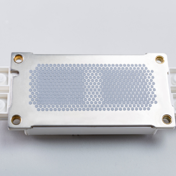
High-Performance Die-Level TIMs (TIM1 / TIM1.5)
Thin, high-performance thermal interface materials are used at the die-level interface, either between the die and an integrated heat spreader (TIM1) or directly between the die and a cold plate in lidless or direct-to-cooling architectures (often referred to as TIM1.5). These interfaces represent one of the most critical thermal bottlenecks in high-power 2.5D and chiplet-based packages.
Integrated Heat Spreader (IHS)
Copper or Cu–Mo–Cu heat spreaders distribute heat laterally while managing CTE mismatch to reduce mechanical stress and warpage.
Power-Aware Die Placement
High-power logic dies are positioned closer to the center of the package to improve thermal uniformity and reduce edge-related gradients.
HBM Thermal Vias & Dummy TSVs
Thermal vias and dummy TSVs improve vertical heat extraction from memory stacks and help mitigate thermal shadowing.
With interface thermal performance defined as a priority, the next consideration is the selection of high-performance TIM1 formats. Thermal interface materials are available in several forms, each offering different trade-offs in bondline thickness control, application method, cycling stability, and compatibility with advanced package geometries such as 2.5D and chiplet architectures.
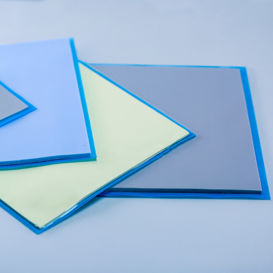
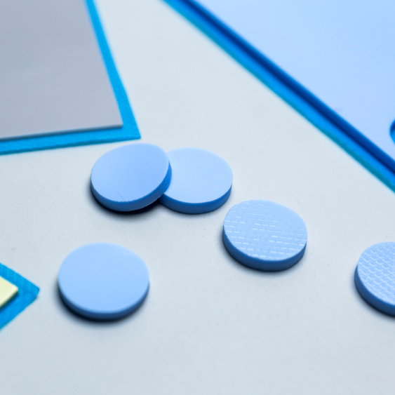
Phase Change Materials
Enable thin, uniform bondlines with stable thermal performance and minimal pump-out.
Thermal Putty Pads
Highly conformable materials designed to accommodate large tolerances and surface flatness variation.
Thermal One-Part Hybrids
Dispense-ready materials supporting high throughput, long-term reliability, and reworkability.
Thermal Gap Pads
Compressible pads that provide electrical insulation and stress relief across uneven interfaces.

Thermal Grease
Easy-to-apply materials offering good initial performance but requiring pump-out validation.
Thermal Two-Part Hybrids
Dispensed systems combining softness, reliability, and long service life.

Why Phase Change Materials are Strong Candidates for TIM1 and TIM1.5 in 2.5D Packages
Among available high-performance TIM formats, phase change materials (PCMs) occupy a practical middle ground for 2.5D IC packages. They combine low interface thermal resistance with controlled bondline formation, limited mechanical compliance, and process compatibility with large-area, thin, and mechanically sensitive package stacks.
In 2.5D architectures, where large die areas, thin lids, package warpage, and non-uniform contact pressure can degrade interface quality, PCMs offer a way to maintain thermal performance while accommodating mechanical variation.
| 2.5D Package Challenge | How Phase Change Materials Address It |
|---|---|
| High local heat flux and thin thermal budgets | PCMs soften at operating temperature to wet surface asperities, forming thin and uniform bondlines with low thermal resistance. |
| Large die area and package warpage | Controlled compliance allows PCMs to accommodate non-uniform pressure and surface flatness variation without loss of contact. |
| Reliability under power and thermal cycling | Compared to greases, PCMs show lower pump-out and migration, maintaining interface stability over time. |
| Need for manufacturability and rework | PCMs can be supplied as films, pads, or printable pastes, enabling controlled placement, automation, and reworkability. |
For large-area, high-power 2.5D packages where thermal resistance, interface uniformity, mechanical variation, and long-term reliability must all be balanced, phase change materials provide a predictable and manufacturable TIM1 solution aligned with both performance targets and package constraints.
PTM7950
Solstice PTM7950 is a high-performance phase change material optimized for low thermal resistance at critical interfaces in high-power packages. It maintains stable performance under thermal and power cycling while supporting scalable, high-volume application. Its polymer-based PCM system softens within typical operating temperature ranges to wet surface asperities, reducing contact resistance and enabling consistently low interface thermal impedance across large die areas.
Key Features
- Ultra-low thermal impedance under typical interface pressures, enabling efficient heat transfer in high-power semiconductor packages
- Silicone-free formulation that eliminates pump-out, bleed-out, and dry-out risks associated with conventional thermal greases
- Industry-proven long-term reliability validated under thermal and power cycling conditions
- Minimum bondline thickness around 20 µm, with typical bondlines below 50 µm for low thermal resistance interfaces
- Designed to operate effectively under interface pressures of approximately 30–40 psi
- Optimized for large-area die and chiplet-based package interfaces requiring uniform thermal contact
Available Versions
- PTM7950 Pad — easy to apply, no drying or curing steps required
- PTM7950-SP — paste version designed for automated stencil printing
- PTM7950-SPS — paste version with a slow-drying solvent for extended open time
The following references provide practical guidance on thermal behavior, interface stability, and long-term reliability when using PTM7950 as a thermal management solution in advanced semiconductor packages, such as 2.5D and chiplet-based architectures.
Thermal Stability (TGA Curve)
Provides thermogravimetric analysis (TGA) data showing the thermal stability and mass loss behavior of PTM7950 across temperature, supporting material selection for high-temperature and long-life semiconductor applications.
Reliability Test Results
Summarizes reliability testing of PTM7950, including HAST (96 h), high-temperature baking (1000 h), temperature cycling (1000 cycles), and double 85 testing (1000 h), demonstrating long-term interface stability under accelerated aging conditions.
PTM6880
Solstice PTM6880 is a high-performance phase change material engineered for next-generation high-power semiconductor packaging. With a bulk thermal conductivity of 6.0 W/m·K and thermal impedance as low as 0.056 °C·cm²/W, it supports highly efficient heat removal in dense electronic assemblies where local heat flux and thermal gradients are significant. Its robust, non-pump-out formulation ensures stable interface behavior under aggressive thermal cycling and mechanical stress. Built on a polymer PCM system with optimized filler loading, PTM6880 has demonstrated reliability through 1000 thermal shock cycles and extended high-temperature aging, making it well suited for mechanically and thermally demanding package environments.
PTM6880 activates at a phase change temperature of approximately 45 °C, allowing the material to conform to surface irregularities, reduce interfacial resistance, and form extremely thin bond lines during operation. This combination of thermal efficiency and interface stability makes PTM6880 an effective choice for advanced, high-power packages where hotspot mitigation and long-term reliability are critical.
Thermal Impedance vs. Pressure
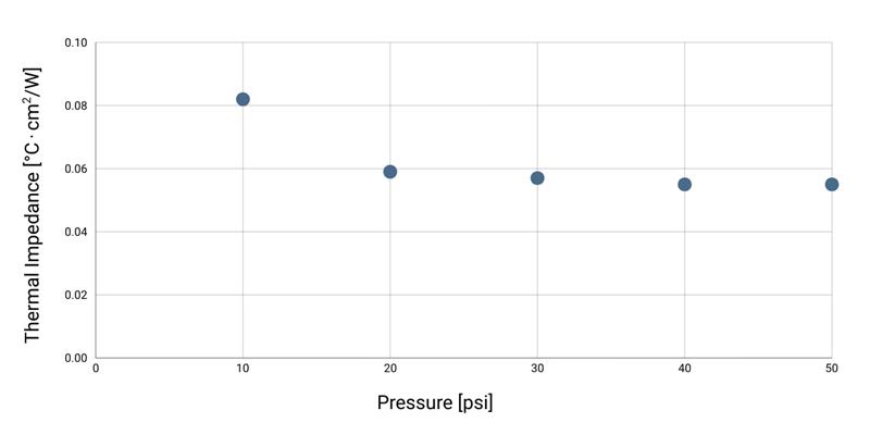
Typical thermal impedance values measured under controlled test conditions.
Key Material Properties (PTM6880)
0.056 °C·cm²/W (ASTM D5470)
6.0 W/m·K (ASTM D5470)
45 °C (DSC)
20 μm (Internal)
2.7 g/cm³ (ASTM D792)
Typical property values shown for reference only and should not be used as specifications.
For detailed specifications, application guidance, and background on PTM6880:
Controlling Warpage with Henkel Loctite Eccobond LCM1000AG-1
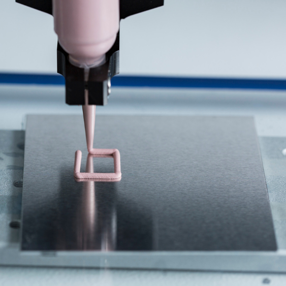
Henkel LOCTITE ECCOBOND LCM 1000AG-1 is an epoxy-amine based encapsulant designed for liquid compression molding (LCM) in advanced wafer-level packaging.
Liquid Compression Molding (LCM) is less stressful on delicate components than traditional transfer molding. In LCM, a precise amount of the liquid compound is dispensed onto the wafer, which is then pressed and cured under controlled conditions. This method:
- Applies lower pressure, which reduces mechanical stress on thin, fragile dies.
- Allows for void-free filling of the fine gaps between dies, crucial for high-density packages.
- Enables fast in-mold curing, increasing manufacturing throughput without compromising the material's integrity.
As an overmolding material, it is particularly valuable for 2.5D packaging, where it helps address key challenges such as warpage control, fine gap filling between closely spaced dies, and overall package reliability. The following are the key features of Henkel LOCTITE ECCOBOND LCM 1000AG-1:
Ultra-Fine Filler
LCM 1000AG-1 is a solvent-free encapsulant featuring ultra-fine fillers, perfect for 2.5D devices that have extremely small gaps between elements. The small filler particles (average size 3 µm, maximum size 10 µm) allow for rapid flow rates and complete trench filling without voids, guaranteeing full coverage, protection, and enduring reliability.
Ultra-Low Warpage
Low warpage inhibits stress accumulation inside the package, guaranteeing that no area experiences excessive compression or tension. Consequently, the package remains whole and provides enhanced long-term dependability, making LCM1000AG-1 a perfect choice for high-density and large-scale 2.5D packages
SVHC-Free Formulation
This formulation helps manufacturers meet strict global environmental rules like the EU's REACH. It simplifies the supply chain by reducing the need for detailed documentation. LCM 1000AG-1 meets the growing demand from consumers and businesses for safe and sustainable products.
High Toughness and Purity
LCM 1000AG-1 is made to be a high-toughness, high-purity encapsulant. This provides strong mechanical support and protection for integrated circuits, further boosting the package's reliability and durability under various operational stresses.
More Information About LCM 1000AG-1

Frequently Asked Questions About 2.5D IC Packaging
What is a "chiplet" and how does it relate to 2.5D packaging?
A chiplet refers to a smaller, functional block of an integrated circuit. It either functions as a CPU, memory or as an input/output. In 2.5D packaging these chiplets are placed side-by-side and are connected to the interposer via microbumps.
How does 2.5D packaging address the limitations of Moore's Law?
2.5D packaging allows for heterogeneous integration and chiplet-focused approach, which means that package performance can be improved without being purely dependent on shrinking transistor sizes, which is restricted by both cost and physical limitations.
In what applications is 2.5D packaging most commonly used?
2.5D packaging is typically used for applications related to high-performance computing. AI accelerators, and high-end CPUs & GPUs. To cater towards increasing demand for HPC, improvements in 2.5D packaging are being developed such as silicon bridge solutions replacing the traditional silicon interposer, glass interposers & designing panel-level packaging.
How is liquid compression molding different from traditional molding methods?
Traditional molding methods involve a pre-measured solid or semi-solid molding compound that is preheated, placed on an open mold cavity, then closed and compressed. On the other hand, liquid compression molding directly injects a liquid material into a heated mold. Traditional molding methods are preferred for larger, simpler packaging designs while LCM is preferred for more intricate, advanced packaging.
Further Reading on 2.5D Packaging Materials


Optimize thermal performance and reliability in advanced 2.5D and chiplet-based packages.
Talk to our engineers about selecting the right materials for your package architecture, thermal budget, and long-term reliability requirements.