
Underfills
Capillary flow and Pre-applied Underfills for Flip chips and BGA arrays
- Home

- Products
- Encapsulants & Underfills
- Underfills
Underfills
Underfills offer the highest levels of reliability with the options of both reworkable and non-reworkable formulations. Materials are available that deliver ultimate processability with fast flow speeds and the capability to effectively fill bottom-side component spaces with extremely low bump heights. Formulations are designed to reduce stress caused by mismatched expansion coefficients, and have outstanding reliability in thermal cycling, thermal shock, drop testing and other demanding tests, as well as in use.
To enhance the reliability of many handheld devices, underfills offer formulations that quickly fill the space between the package and board, cure fast, offer outstanding protection for solder joints against mechanical strains such as shock, drop and vibration, and allow for reworkability. When full underfill is not required, cornerbond and edgebond technologies provide a cost-effective solution, with strong perimeter reinforcement and self-centering capability.


LOCTITE ECCOBOND UF 9000AE
- Low die warpage
- Best large die underfill
- 260°C reflow capability for Pb- free, low-k applications
- In stock


LINQBOND UF3501R | Reworkable Underfill
- Low Viscosity
- High elasticity, fatigue and crack resistant
- One-component, solvent-free
- 16 weeks

LINQBOND UF3550R | Reworkable Underfill
- Low stress, high fatigue and crack resistance
- Low viscosity, solvent-free
- Fast cure
- 16 weeks


LOCTITE ABLESTIK NCF 234
- Non-conductive Underfill Film
- Enable fine pitch, narrow gap Cu Pillar
- Pb-free & low κ
- 48 days

LINQBOND UF-1170 | Liquid Epoxy Underfill for BGA/CSP
- Single component
- Excellent heat and moisture resistance
- Automotive grade
- 12 weeks

LOCTITE FP4804 | Epoxy Underfill
- Good flowability
- Low CTE/modulus (reduced stress)
- No resin bleed out on glass
- 12 weeks

LOCTITE ECCOBOND UF 3578
- Fast heat-cure adhesive designed for underfill and fixture applications
- Thixotropic and fluorescent for controlled flow and optical inspection
- Reflow-compatible for SMT processes
- 12 weeks


LOCTITE ECCOBOND E 1216M
- Snap Cure
- Non anhydride curing chemistry
- Excellent adhesion and strength
- 40 days


Product Selector Guide
| Product | Description | Viscosity (MPa-s) | Glass transition temperature (°C) | CTE a1 | CTE a2 | Cure time (min) | Cure Temp °C | Available | Key attributes |
|---|---|---|---|---|---|---|---|---|---|
| Board level Underfills | |||||||||
| LINQBOND UF3801 | Reworkable, and solvent-free, one-component epoxy underfill | 250 | 103 | 64 | 253 | 10-20 | 130 | Yes |
|
| LINQBOND UF3802 | Reworkable, and solvent-free, one-component epoxy underfill | 290 | 113 | 88 | 252 | 10 | 130 | Yes |
|
| LINQBOND UF3501R | One-component epoxy adhesive | 3,250 | 50 | 30 | 177 | 30 | 80 | Yes |
|
| LINQBOND UF3550R | Reworkable one-component epoxy adhesive | 700 | 35 | 60 | 215 | 30 | 80 | Yes |
|
| Loctite 3508NH | Reworkable cornerbond | 70,000 | 118 | 65 | 175 | - | 245 | Yes |
|
| Loctite 3517M | Reworkable underfill for solder joint protection | 2,600 | 101 | 65 | 191 | 5 | 120 | Yes |
|
| Loctite ABLESTIK ACP 3122 | Anisotropic epoxy adhesive (Z axis) | 22,000 | 100 | - | - | 5 seconds | 150 | Yes |
|
| Loctite ECCOBOND E1172A | Non reworkable capilary underfill | 17,000 | 135 | 27 | 85 | 6 | 135 | Yes |
|
| Loctite ECCOBOND E1216M | Capillary flow epoxy underfill | 4,000 | 125 | 35 | 131 | 4 | 150 | Yes |
|
| Loctite ECCOBOND FP4502 | Single component liquid epoxy underfill | 35,000 | 115 | 22 | 84 | 30 | 165 | Yes |
|
| Loctite ECCOBOND FP4526 | Liquid epoxy capillary underfill | 4,700 | 133 | 33 | 101 | 15 | 165 | Yes |
|
| Loctite ECCOBOND FP4527 | Epoxy capillary underfill | 12,000 | 158 | 26 | 87 | 15 | 165 | Yes |
|
| Loctite ECCOBOND FP4530 | Snap curable fast flowing Underfill | 3,500 | 145 | 46 | 150 | 7 | 160 | Yes |
|
| Loctite ECCOBOND FP4531 | Snap curable non reworkable underfill | 10,000 | 161 | 28 | 104 | 7 | 160 | Yes |
|
| Loctite ECCOBOND FP4549 | Underfill for IC passivation materials | 2,300 | 140 | 45 | 143 | 30 | 165 | Yes |
|
| Loctite ECCOBOND UF1173 | One component void free underfill | 7,500 | 160 | 26 | 103 | 5 | 150 | Yes |
|
| Loctite ECCOBOND UF3578 | One-component, heat-curable epoxy underfill | 55,000 | 121 | 39 | 138 | 10 | 120 | Yes |
|
| Loctite ECCOBOND UF3810 | Reworkable epoxy underfill | 394 | 102 | 55 | 171 | 8 | 130 | Superseded by UF3811 |
|
| Loctite ECCOBOND UF3811 | Reworkable epoxy underfill | 354 | 124 | 61 | 190 | 30 | 110 | Yes |
|
| Loctite ECCOBOND UF3812 | Reworkable epoxy designed for CSP,WLSCP and BGA | 350 | 131 | 48 | 175 | 10 | 130 | Yes |
|
| Loctite ECCOBOND UF3820 | Reworkable epoxy designed for CSP,WLSCP and BGA | 340 | 133 | 51 | 172 | 10 | 130 | Yes |
|
| Loctite ECCOBOND UF3915 | Reworkable underfill designed for WLSCP and flip chip | 5,500 | 125 | 25 | 100 | 7 | 160 | Yes |
|
| Loctite ECCOBOND UF8806G | Cyanate ester with superior adhesion | 4,500 | 136 | 27 | 97 | 45+60 | 195 | Yes |
|
| Loctite ECCOBOND UF9000AE | Designed for large die flip chip BGA and Cu Pillar | 9,082 | 111 | 23 | 85 | 15+90+15+120 | 165 | Yes |
|
| Semiconductor Underfills | |||||||||
| LINQBOND UF1170 | BGA/CSP solder joint | 10,000 | 190 | 31 | 105 | - | - | Yes | |
| LINQBOND UF3803 | Designed for flip-chip packaging | 7,000 | 80 | 25 | 133 | 30 | 150 | Yes |
|
| Loctite ECCOBOND FP4804 | Flip-chip and BGA components | 102,000 | 51 | 15 | 53 | 30 + 120 + 30 + 60 | 100 + 150 | Yes |
|
| Loctite ECCOBOND FP5201 | BMI/Acrylate for flip chip | 21,000 | 171 | 31 | 65 | 30 | 165 | Yes |
|
| Loctite ECCOBOND NCP5209 | Non conductive paste Underfill | 12,500 | 145 | 28 | 80 | 30 + 120 | Ramp to 160 | Yes |
|
| Loctite ABLESTIK NCF218 | Non conductive underfill film | - | 119 | 24 | 190 | 30 + 60 | Ramp to 175 | Yes |
|
| Loctite ABLESTIK NCF234 | Non conductive underfill film | - | 105 | 42 | 138 | 30 + 120 | Ramp to 175 | Yes |
|
| Loctite ECCOBOND UF8830S | Liquid epoxy capillary underfill for BGA | 22,120 | 118 | 25 | 100 | 30 + 120 | Ramp to 150 | Yes |
|
Frequently Asked Questions
Frequently Asked Questions about Underfills
Do you have a Pre-Applied Underfill?
Yes, Loctite Eccobond NCP5209 is a pre-applied underfill for fine-pitch Cu pillars and Cu OSP flip chip devices. This is a non-conductive paste underfill that makes use of a thermo-compression (TC) bonding process to provide a robust and complete bump protection. NCP 5209 is typically used for die sizes ranging from 4x4mm to 12x12mm with bump pitches less than 100 µm and gaps less than 40 µm for a high-reliability result.
Is there a "no flow underfill" that can be used with standard reflow oven?
We used to promote this "fluxing underfills" around 10 years ago but without success. The process window appeared to be too small for robust performance. Also, the introduction of vacuum and pressure ovens improved the performance of such underfills, hence we stopped these pre-applied underfills for devices with solder bumps. Instead, a partial POST applied underfill Loctite Eccobond UF 1175 which can be considered which provides good UPH and reliability.
Learn More
Semiconductor and Board-Level Underfills
Underfills are (mostly) epoxy based thermo set materials that contain (mainly) silica fillers and are designed to flow in the gap between the board and the component. They are typically applied after solder reflow and require heat cure.
Underfill materials need to have a low viscosity to allow them to flow under the components by capillary force. Substrate heating is also sometimes required to facilitate a good flow process and allow the capillary force to pull the underfill under the package.
Underfill Properties
Thermally, underfills increase the thermal package reliability by distributing the stress across the surface of the die or substrate instead of being concentrated in the solder balls especially during thermal cycling (TC). It is important to point out that the peripheral (outside) bumps are stressed the most.
Mechanically, it is used to increased mechanical shock resistance in various configurations such as button push, drop resistance and bending. Specifically for drop performance, the UF properties provide exquisite improvement.
Finally, underfills reduce moisture absorption and chemical contamination. Moisture can create dendrite formations that would result in electrical shorts and create bridges in places where traditional conformal coatings wouldn't be able to penetrate.
Board-Level Underfills
Underfills come in two types. Semiconductor (die) level and board level. The board level types are the ones applied between the finished IC package (ie BGA) and the PCB.
There are three main types of board level underfills:
Full Capillary Underfill
- Dispense material along edge(s), completely flows under the component
and fills the complete space - Improved thermal and mechanical reliability
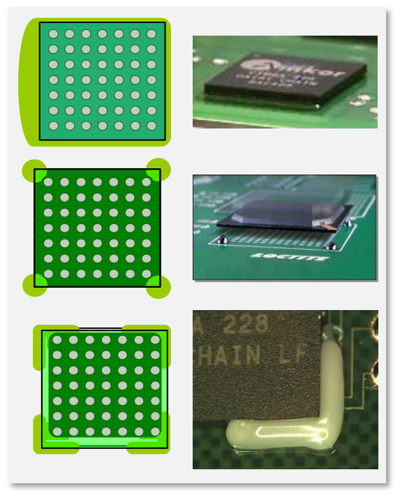
Partial Underfill - Corner Bond
- Dispensed before reflow
- Dispense dots or “L” shape only at the corners
- Small improvement in mechanical reliability, not in thermal reliability
Partial Underfill - Edge Bond
- Dispense after reflow
- Only covers corner fillets
- Small improvement in mechanical reliability, not in thermal reliability
- Can be UV or thermal Cure.
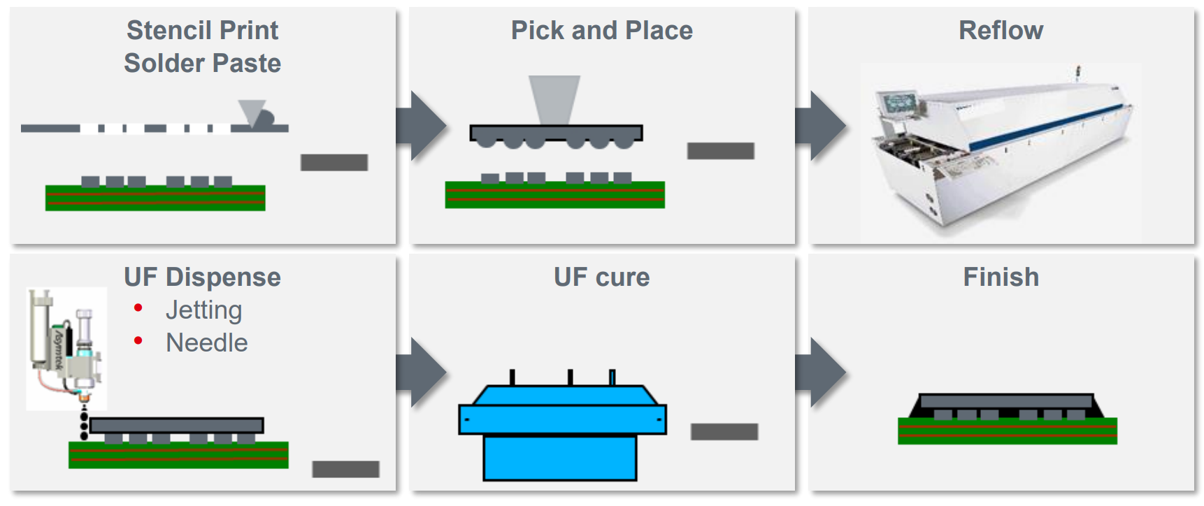
Standard Capillary Underfill Process
Capillary underfills have a pretty standard operational process. They are applied and cured post reflow so they don't have to withstand extremely high temperatures. The common steps one would have to follow are:
- Stencil print with solder paste
- Pick and place the die on the board
- Take the package through the Reflow oven
- Dispense the underfill by either jetting it or with a classic syringe
- Cure the underfill for the recommended time and temperature
- Done. You have a thermally, mechanically and environmentally protected semiconductor package
Preparing the Substrate
Before applying the underfill we need to prepare the substrate for the application. As a first step we need to clean the substrate with either solvent wash or plasma to improve the surface tension and reduce flux residues.
Afterwards we prebake the board to remover the moisture and any remaining solvents. Normally this is not needed after reflow but it can be a necessary step when we had the boards stored for long, in order to remove the moisture trapped in the board/components that can create outgassing voids when curing.
Heat that is typically in a range between 60°C and 100°C can reduce the viscosity and the surface tension while improving the wetting properties of the substrate.
Developing a Capillary Underfill Process
Of course it is not as simple as it sounds (is it ever?). In order to find the ideal underfill process there is a series or steps you need to take to optimize it.
To begin with we need to calculate the required volume: L x W x H (gap) in mm. Using this value, times the specific gravity (can be found in the TDS) we get the volume measured in mg. Granted this is a rough calculation, not taking into account the solder bumps, but it is good enough.
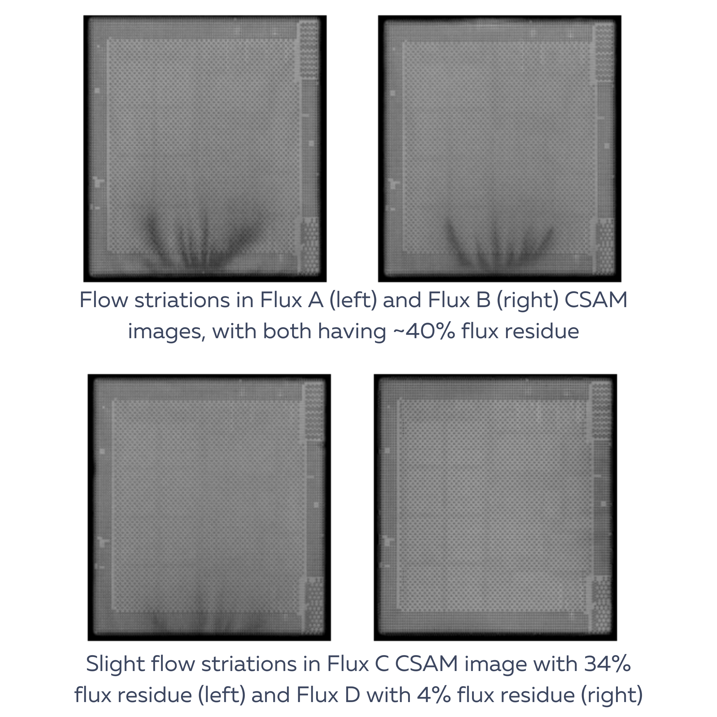
Let's say that the calculated volume is 10mg. In this case we start with passes of 1 mg. Dispense 1 pass and wait until the material is under the component, dispense second pass... proverbially rinse and repeat. When the underfill is creating a fillet on the opposite site than the component is finished. Now it is the time to check the underfill quality by flat and X sections.
Next step is to reduce the amount of passes to check the maximum possible speed. Flow out and top die contamination should be the main points of focus and concern . If needed, changing hardware can also be a solution. A small nozzle can result in an unstable dispense process. With jetting the flowrate is determined by the dot weight, so the machine will calculate the amount of dots needed for the programmed dispense pass. For needle dispensing the flowrate is calculated by the amount dispensed per second. The robot speed will be adjusted to ensure the right volume per pass is dispensed.
Dispensing
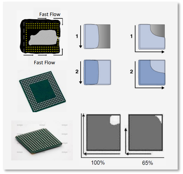
The dispensing pattern needs to be optimized to avoid air encapsulation. There are I, L and U shaped dispense patterns with one or multiple passes. U is the most dangerous for void entrapment and should be carefully considered. These parameters depend on the ball grid layout.
The main challenge is to make the process as quick but also as good as possible, with quality always coming before speed. Avoiding the overflow and contaminating adjacent components is the main target for this process. A bigger amount per pass will give a faster process but a bigger flow out, so a compromise has to be made between how good an underfill needs to be and how fast you can apply it. Any flow out can impact volume repeatability and create solder extrusion so it is always advised to optimize it and have a dispense system with a built in weight scale for volume control.
Curing
Curing of the Underfill should occur as soon as possible after dispensing since moisture absorption becomes a bigger risk after a couple of hours. Also because of the filler settling we might need a gelling step to increase viscosity.
Thermal mass of the boards and components should be taken into account when settling the curing process. Keep in mind that the curing time and temperature in the TDS are guidelines that don't take the thermal mass into account. Testing needs to be done with thermo couples under the device to track time and temperature and be done with a full oven since the thermal mass will be massively different with one board and with a full oven. As a general rule, over-cure is not possible with time.
Application Notes & Troubleshooting
Presentations
Underfills, Introduction and Product Propositions
This presentation provides an introduction to underfill materials used in advanced electronic packaging and semiconductor assembly. It explains the purpose of underfills, their role in improving mechanical reliability and thermal cycling performance, and the different underfill technologies available. The presentation also highlights key product propositions and selection considerations to help optimize performance in high-density electronic applications.
Related Blogs

Why Do We Need Reworkable Underfills?
This blog discusses why reworkable underfills are necessary & CAPLINQ’s product offerings for reworkable underfills,

