Diodes
Axial, Schottky and SOD
-
Home

-
Semiconductors
- Diodes
Diodes
Diodes Portfolio
A diode is two-terminal electronic component that conducts current flow in only one direction and restricts current from the opposite direction with a P-N Junction or an alternative junction. Think of it as a “one-way street” for electric current. Shown below is classification of diodes by structure.
The PN junction of diode, is formed by joining two doped regions of semiconductor material, one p-type and one n-type. The type of doping determines whether the material has an excess of positive or negative charge carriers.
The different types of diodes in the image have different structures and properties, which makes them suitable for a variety of applications. For example, rectifier diodes are used to convert alternating current (AC) to direct current (DC), while Zener diodes are used to regulate voltage and some for signal modualtion isolation, stabalization and signal gating.
On the other hand, Metal semiocnductor junction is categorized into two: Schottky barrier diodes are another type of diode with a different structure, which uses a junction betwwen meatal and lightly dopes semiconductor instead of a p-n junction. This gives them some unique properties, such as a lower forward voltage drop. Secondly a junction betwwen a metal and heavily doped semicnductor that behaves as low resistance ohmic contacts (basically electrical shorts) that have significant influence on different devices and on the performace of high-speed transistors.
WHAT ARE DIODES USED FOR?
-
REVERSE CURRENT PROTECTION: Diodes allow current to flow in only one direction, protecting components from damage due to reverse current. For instance, they prevent a battery from being discharged back into the charging circuit.
-
SIMPLE VOLTAGE REGULATORS : By exploiting the voltage drop across the diode, which is relatively constant, diodes can be used in simple voltage regulator circuits to maintain a steady output voltage.
-
VOLTAGE STABILIZERS: Zener diodes, a special kind of diode, can be used as voltage stabilizers or references by maintaining a constant voltage over a wide range of current flows.
-
CONVERTING AC TO DC: Diodes are used in rectifier circuits to convert alternating current (AC) to direct current (DC). A full-wave rectifier, for example, uses multiple diodes to convert both halves of an AC waveform to pulsating DC
Each of these applications takes advantage of the diode’s fundamental property: allowing current to flow freely in one direction while offering high resistance in the other. This principle is key to many electronic circuits and devices
HOW DOES A DIODE WORK?
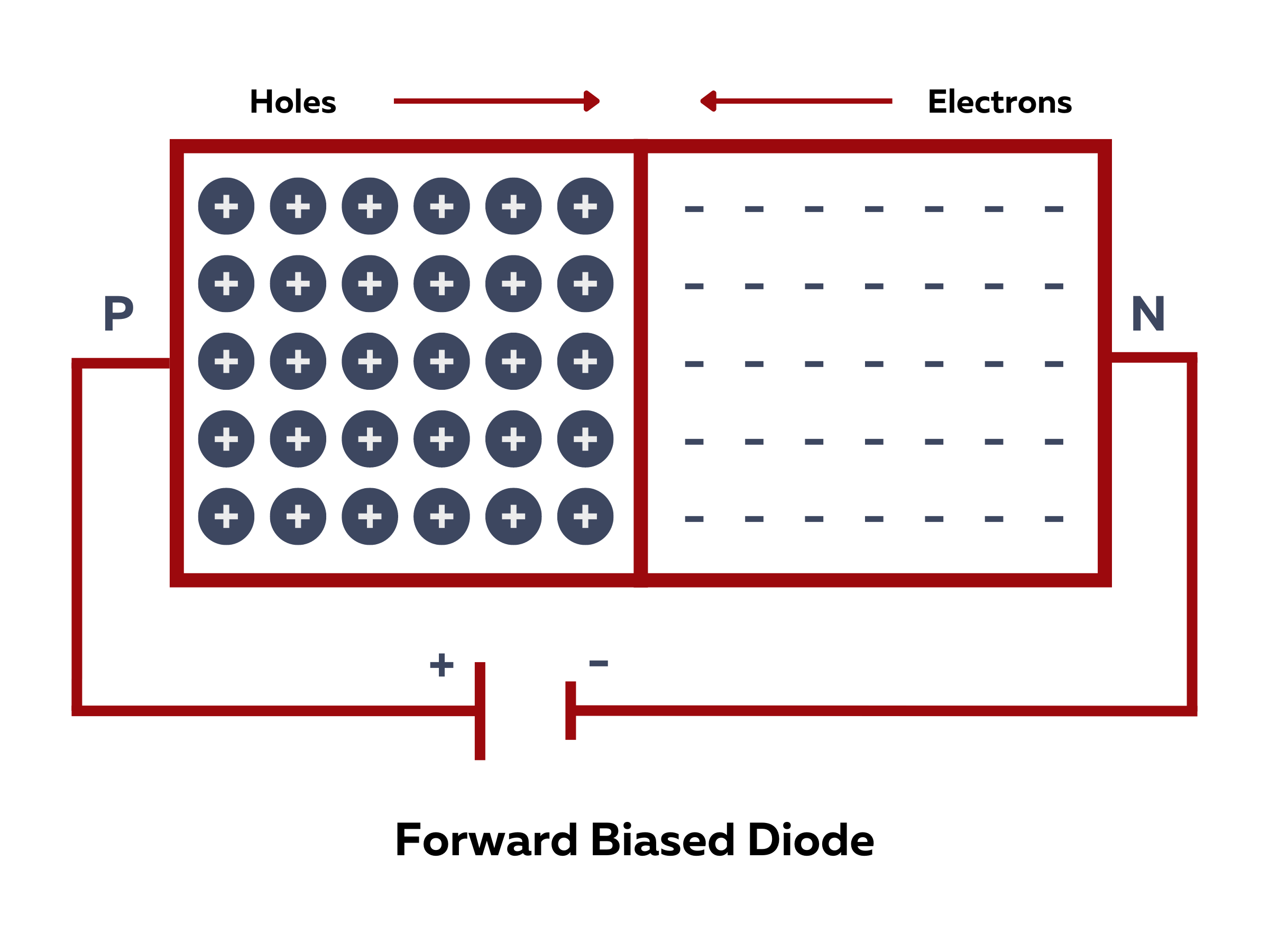
To fully understand how a diode works, basic concept of coventional flow theory should be understood. In coventional flow theory, current flows from the positive terminal of the battery to the negative terminal, as electron moves it leaves 'holes' behind. The holes are said to travel in the opposite direction from the electrons in the conductor.
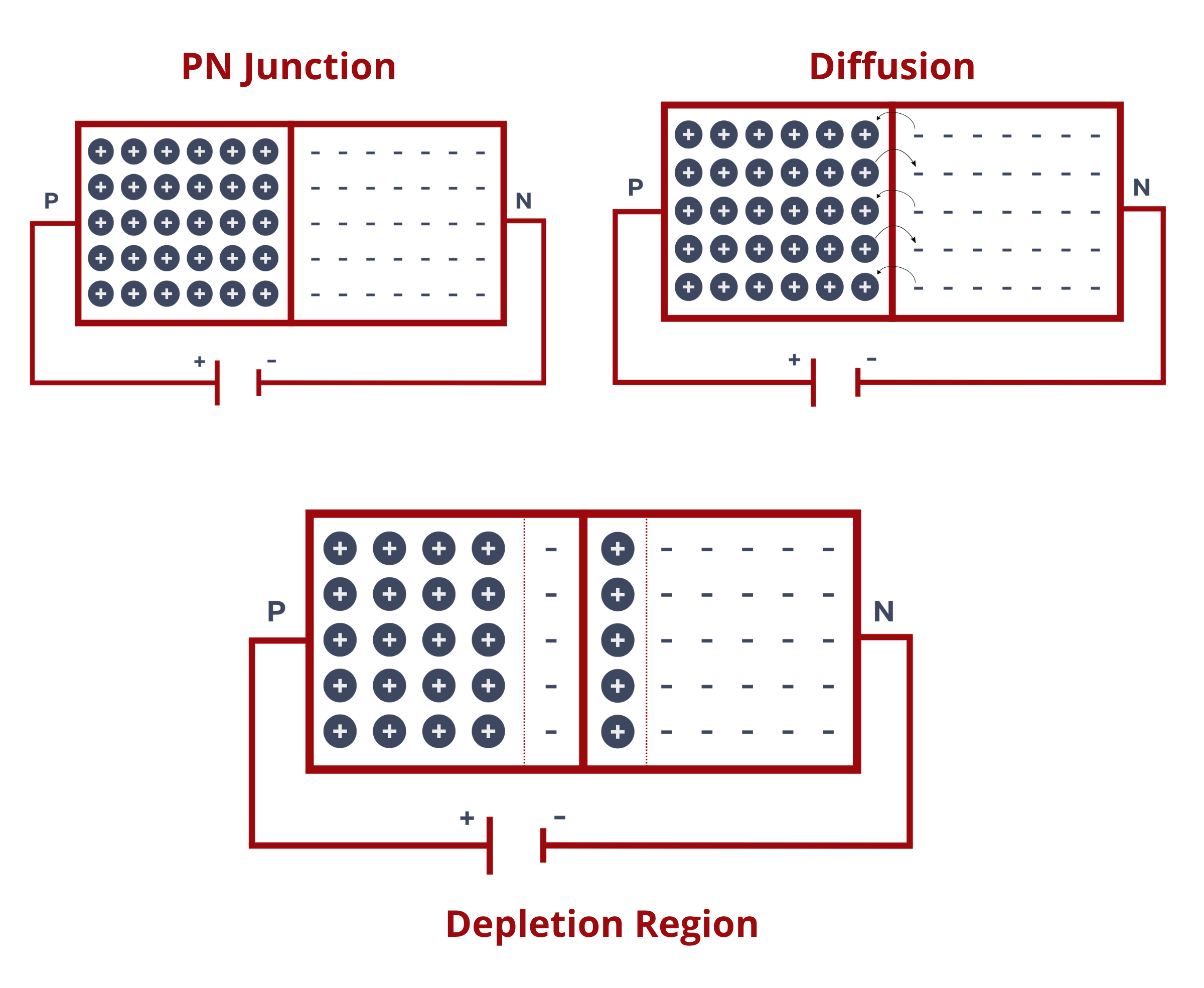
For a diode to block current in one flow and pass current in the opposite direction, joining a P type material with N-type material thus creating a PN junction at their boundary layer. The basic mechanism at the PN junction can be descrive as follows:
-
Diffusion: The n-material has electrons as charge carriers and p-material has holes (places depleted of electrons) as charge carriers. Due to the concentration gradient, holes from the P-region and electrons from the N-region start to diffuse into each other's region.
-
Formation of the Depletion Region: As the electrons and holes meet, they recombine and neutralizes each other. This leaves behind charged ions, creating a neutral region devoid of charge carriers called the depletion regio, prevents further electron flow.
-
Built-in Potential: The recombination process creates a potential difference across the junction, called the built-in potential. This potential opposes further diffusion.
-
Equilibrium: The diffusion and drift of charge carriers reach a dynamic equilibrium. The depletion region extends deeper into the N-region due to the higher mobility of holes in the P-region.
Key Concepts
Forward-biased Condition: When an external voltage is applied such that the P-region is connected to the positive terminal and the N-region to the negative terminal, overcoming the built-in potential, allowing charge carriers to move across the junction.
Reverse-biased Condition: When an external voltage is applied in the opposite direction, the built-in potential increases, widening the depletion region preventing charge carriers from moving across the junction.
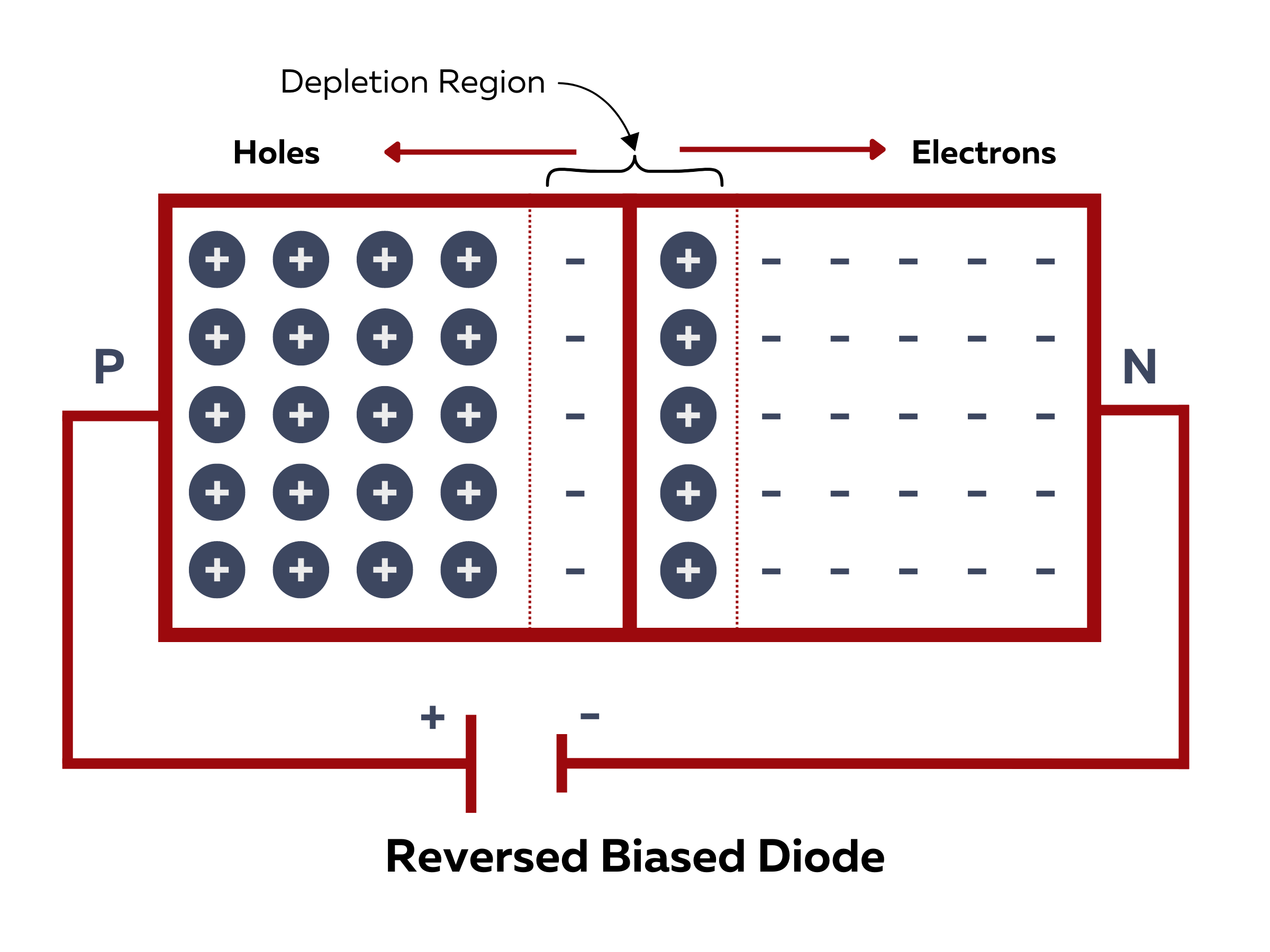
Reverse Bias Leakage: Ideally, any device should not conduct any current under reverse bias but due to minority carriers generated by thermally induced electron-hole pairs, small current flows. However for most practical purpose, this leakage current is negligible and effectively ignored, typically around 1 mA for Germanium diodes and 1 µA for Silicone diode. It only becomes significant when the reverse voltage reaches the breakdown voltage thereby causing an avalance of current flow. Moreover, there are other paths for leakage aside from through the PN junction itself such us through the surface leakage, where surface-leakage current is also directly proportional to the reverse voltage.
Breakdown Voltage is the largest reverse voltage that can be applied in a diode without causing an exponential increase in leakage current. It can also be defined as the minimum volatge required to violate a diode and forcing a current through it. It is not destructive in nature but if there is nothing in series with the diode to limit the maximum current through it, it could be damaged by overheating. Useful most often as voltage reference.
Hysol and LINQSOL EMC Selection Guide for Discrete Through-Hole Devices
This guide helps identify suitable epoxy molding compounds for discrete through-hole devices based on package family, voltage and temperature class, thermal load, leadframe interface, and reliability target. The highlighted rows at the bottom distinguish extended portfolio options used when requirements escalate toward fullpack insulation, higher thermal conductivity, high-power TO packages, or SiC/GaN device reliability.
| Product | Key Benefit | Typical Use Case |
|---|---|---|
| Hysol KL-G100L | Cost-driven general-purpose solution High-throughput option with strong mold flow characteristics for volume diode production |
Axial diode packages where moldability, high-volume processing, and stable encapsulation around axial leads are primary selection triggers |
| Hysol GR260 | Balanced diode solution Mainstream diode position for balanced electrical reliability, moldability, and cost performance |
Axial diodes and bridge rectifiers where high-voltage reliability, stable molding behavior, and practical production cost must be balanced |
| Hysol GR260-SL | Stress-control focused solution Reliability-driven, low-stress option for packages where cracking, delamination, or thermal cycling sensitivity must be controlled |
Axial diodes, bridge rectifiers, and selected TO packages where mechanical stress control and long-term reliability are stronger drivers than maximum thermal conductivity |
| LINQSOL EMC-G135 | Balanced rectifier-focused solution Combines moldability, low-stress behavior, and moderate thermal performance for rectifier-style packages |
Bridge rectifiers such as GBU, KBJ, GBS, and related rectifier or SMX packages where cost-effective thermal performance is required |
| Hysol GR360A-ST | Throughput-focused option Supports broad through-hole package compatibility where process economy and molding robustness are important |
TO, diode, PDIP, SIP, and related through-hole formats where low cost of ownership, moldability, and broad process fit drive selection |
| Hysol GR300 | Electrical reliability and leadframe compatibility Positioned for TO power packages requiring HTRB performance and adhesion to nickel leadframes |
TO-220, TO-247, and related TO power discrete packages where Ni leadframe compatibility and reverse-bias reliability are key selection triggers |
| Hysol GR30HT | Thermal performance upgrade for power packages Provides an escalation path for TO packages requiring improved heat dissipation with reliable high-temperature electrical performance |
TO-92, TO-220, TO-247, TO-3P, and related power discrete packages where heat dissipation, HTRB, TCT, and Ni adhesion become stronger selection drivers |
| Hysol GR750 | High reflow reliability solution High Tg and low-moisture-absorption position for high-power packages with elevated thermal and electrical reliability demands |
High-power TO and advanced discrete packages, including SiC and GaN devices where high-temperature stability and moisture reliability drive material screening |
| Extended portfolio options for advanced power requirements | ||
| LINQSOL EMC-5013 | High thermal conductivity and insulation performance Consider when the request shifts toward fullpack insulation, low porosity, and higher thermal conductivity requirements |
TO-220F, TO-3PF, and fullpack power packages where electrical isolation, heat dissipation, and reliable encapsulation of insulated power devices are central requirements |
| LINQSOL EMC-G375 | Mid-to-high thermal performance solution Improves heat dissipation for TO, bridge, and high-current packages without moving to high-end SiC/GaN materials |
Bridge rectifier, TO power, fullpack, and high-current discrete packages where improved thermal conductivity becomes a dominant selection driver |
| LINQSOL EMC-7535MF | High-voltage and high-power reliability solution Designed for high Tg, low stress, low moisture absorption, and CTI-focused performance |
High-power TO, SiC/GaN, IGBT, and high-voltage discrete packages where elevated thermal, electrical, and moisture-reliability demands drive material screening |