Wafer level packaging
Liquid compression molding & Backside protection films
- Home

- Products
- Encapsulants & Underfills
- Wafer Level Packaging
Wafer Level Packaging
Wafer-level Chip Scale Packages (WLCSPs) are key enablers of smaller, thinner, higher functionality devices that are driving advances in mobility, integration and expansive connectivity (IoT). The mobile phone market has been the primary catalyst for the growth in WLSCP packages in recent years, highly benefiting from the thinner, higher-density ball count capabilities of modern-day WLCPS. The trend toward prolific connectivity through new wearable devices, among other technologies, help maintain the growth rate of WLCSPs.
With the decreasing dimensions and finer ball pitches come increasing wafer processing and handling challenges. Die chipping and cracking, wafer warpage and damage during the SMT placement process onto the PCB substrate are all potential obstacles that have to be overcome for high-yield WLCSP production. Recent advances in film technology have resulted in a new class of materials that help alleviate some of the traditional obstacles with handling and reliability of WLCSPs. Novel backside protection (BSP) films offer packaging subcontractors a technique that helps reduce mechanical damage, while improving laser marking performance and reliability. Additionally, the latest development of liquid compression molding compounds with minimum warpage can be used to map mold and package the chip on the wafer level; opening new pathways to completely reform and reintroduce the way IC packaging is being done.


Product Selector Guide
| Product | Description | Cure Schedule | Tensile modulus @25°C (GPa) | Glass transition temperature (°C) | CTE a1 | CTE a2 | Key attributes |
|---|---|---|---|---|---|---|---|
| Liquid molding compound | 5m @120°C + 1h @150°C | 16 | 158 | 6 | 16 | -Ultra low warpage -CTE matches Silica | |
| Liquid compression molding compound | 10 min @120°C + 1 hour @150°C | - | 135 | 8 | 18 | -High purity -Low stress, ultra-low warpage | |
| LOCTITE ABLESTIK BSP 100 | Back Side protection film | 30m ramp 150°C + 1h @150°C | 8.5 | 162 | 40 | 120 | -Laser markable -MSL1 for WLCSP |
Frequently Asked Questions
Is Wafer Backside Protection only available in film form?
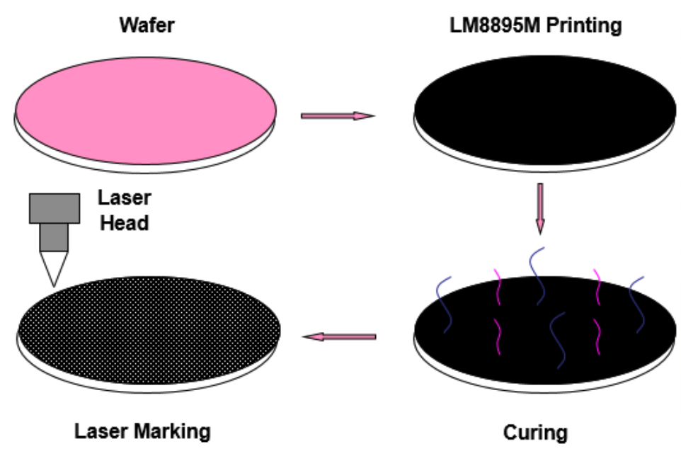
Even though films are the most popular wafer backside protection option, there are also stencil printable liquids that can work for WLCSP laser marking. Products such as LM 8895M are solvent-based epoxies with tiny filler cuts (5um) that exhibit excellent adhesion to silicon and can be laser marked.
How does wafer packaging work compared to traditional processes?
The traditional packaging process flow starts with dicing the wafer and then moving forward with the packaging. Wafer-level packaging skips these process steps by packaging everything while still on the wafer and then dicing individual, ready-to-go packages.
What are the main benefits of using LCM for WLP?
LCM excels at creating very thin and reliable WLP packages. The pressure during molding ensures good encapsulation and eliminates air voids, leading to high-density, reliable electronic components.
What are the limitations of using LCM for WLP?
LCM requires expensive, complex molds designed specifically for the WLP layout. Additionally, not all molding materials work well with LCM due to viscosity limitations. Wafer warpage during molding process can also be a challenge.
Learn More
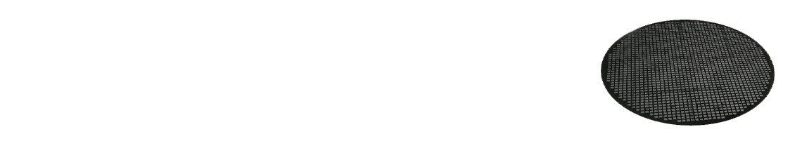
Back Side Protection
Backside protection products are designed for wafer level chip scale packages such as WLCSP and Fan-in. They aids laser marking, protect the chip and improve the reliability of the package. There are two main application methods. One of them is stencil printing with a paste and the other one, that we are going to talk about here, is the lamination with a B-staged film. The film option has been the preferred weapon of choice for key industry players and hence it is our current focus.
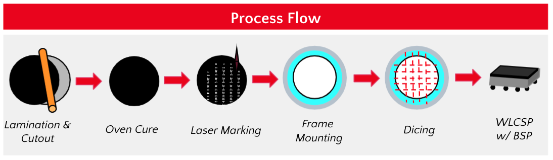
BSP film application process
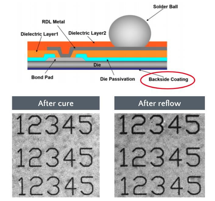
The BSP film application process is simple and allows use of established lamination and dicing equipment. BSP film is laminated onto the wafer, heat cured and laser marked. Dicing tape is then applied prior to die singulation. It is a clean, dry process and allows for elimination of the fillet, while limiting outgassing and bleed. BSP films can accommodate various bondline requirements and help eliminate the need for subsequent mold compound processes. The materials are black in color, which not only promote high visibility of laser markings, but also serve to block light and provide surface protection, helping to keep the circuit surface free from any handling damage.
Backside protection films display excellent reworkability on both 8” and 12” wafers. In the event that the film needs to be removed from the wafer, they are easily peeled off the wafer, leaving no residue. The packaging subcontractor can then reapply the film as per the process noted above. Other competitive materials, particularly with respect to 12” wafers, have shown removal difficulty which can result in wafer damage or the requirement for subsequent cleaning steps.
Laser marking and warpage performance
B staged films exhibit excellent laser marking performance both prior to cure and after reflow, as shown above. This is critical, as the device ID is essential to inventory management, quality control and process tracking.
Warpage performance is also an advantage. After reflow, the material shows less than half the warpage exhibited by competitive materials. It has little thickness change from pre-cure to post-cure, delivering stability and uniformity. Films such as BSP 100 pass MSL1 (3x reflow), thermal cycling testing of 500 hrs., pressure cooker testing (PCT) of 168 hours with excellent adhesion after cure and no delamination after thermal cycling.
While WLCSPs have been part of the miniaturisation conversation for years, their ability to push dimensional limits has been inhibited by handling and processing challenges. Henkel’s new LOCTITE ABLESTIK BSP 100 sets the stage for improved WLCSP reliability and product integration, overcoming past obstacles and enabling future development.
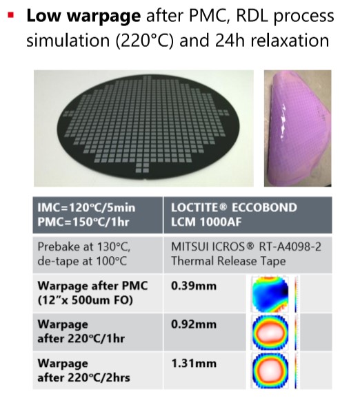
Back Side protection materials are not the only wafer level protection option that we have available. There is also liquid wafer level encapsulation for wafer molding with and without Redistribution layer. This is a development that has been driven by long term REACH compliancy and ultra low warpage needs. You can find information about it in the LCM 1000AF product page. A novel liquid, anhydride free, wafer level molding compound with focus on WLCSP and high density fan out applications.
Liquid Compression Molding
Wafer level packaging (WLP) demands a balance between protecting delicate chips and achieving high-density integration. Liquid compression molding (LCM) emerges as a powerful technique that combines the benefits of both liquid molding and compression molding for WLP applications. LCM leverages a liquid molding compound (LMC) similar to standard liquid molding. However, it incorporates a controlled compression force during the encapsulation process.
Advantages of LCM:
- Improved Thinness: LCM excels at creating very thin packages due to the controlled application of pressure during molding. This is crucial for achieving high-density integrations in modern electronics.
- Uniformity: The pressure ensures consistent material distribution around the die, leading to more uniform electrical characteristics across the entire wafer.
- Reduced Chip Stress: LCM utilizes a significantly lower pressure, minimizing stress on the chips and preventing potential damage.
- Improved Warpage Control: The controlled compression force in LCM helps counteract the warpage that can occur due to the mismatch in thermal expansion between the chip and the encapsulant.
- Faster Cycle Time: The floability of the LCM allows for faster Filing of cavities compared to traditional compression molding.
- Superior Conformal Coating: The liquid nature of the LMC ensures excellent flow and complete coverage around chips and intricate features.
- Cost-Effective: LCM can be a cost-effective option for high-volume production due to its relatively fast cycle times compared to other WLP encapsulation methods.
Related Blogs

Overmolding Solutions
This blog discusses 2.5D Packaging and features LCM 1000AG-1, CAPLINQ & Henkel's overmolding solution for advanced wafer-level packaging.

