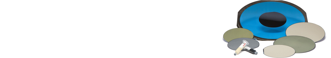
Wafer backside coating
Wafer backside coating for wirebond laminate and leadframe packaging
- Home

- Products
- Die Attach Materials
- Wafer Backside Coatings
Wafer Backside Coatings
Wafer backside coating materials allow for screen or stencil printing of the paste across the entire wafer in a single stroke, increasing throughput by eliminating the need to individually dispense dots of adhesive.
Wafer backside coating provides consistent bond lines and small, controlled fillets which are particularly effective for attaching small die in miniaturized packages and challenging structures like chip on lead where the die pad is smaller than the die. It enables process speed, thickness control and material uniformity and it is critical for die attach applications where fillet control is critical.


LOCTITE ABLESTIK 8008
- Snap curable after B stage
- Low modulus
- Void free bondline without bleed
- No longer available


DMI-3006 Negative Type Solvent Developed Photosensitive Modified Polyimide Stress Buffer Coating
- No warpage of silicone wafer
- UV cured, no hard bake required
- Excellent dielectric properties
- 2 weeks
Product Selector Guide
| Product | Description | Viscosity | Thixotropic index | Tensile modulus @25°C | Glass transition temperature (°C) | CTE a1 | CTE a2 | Key attributes |
|---|---|---|---|---|---|---|---|---|
| Loctite Ablestik 8008 | Ag-filled, die attach wafer backside coating adhesive | 48,000 | 2.6 | 5,451 | 270 | 42 | 67 | -Snap curable after B stage -Low modulus -Void free bondline without bleed |
| Loctite Ablestik 8008HT | Ag-filled, die attach wafer backside coating adhesive | 50,000 | 4.0 | 6,662 | 264 | 37 | 62 | -Thermally conductive -Low modulus -Stencil printing |
| Loctite Ablestik 8008MD | Ag-filled, die attach wafer backside coating adhesive | 67,500 | 2.6 | 3,880 | N/A | N/A | N/A | -Thermally conductive -Low modulus -Good substrate wetting |
| Product | Description | Viscosity | Thixotropic index | Tensile modulus @25°C | Glass transition temperature (°C) | CTE a1 | CTE a2 | Key attributes |
|---|---|---|---|---|---|---|---|---|
| Loctite Ablestik 8006NS | Alumina/silica-filled, epoxy die attach wafer backside coating adhesive | 55,000 | 1.3 | 4,376 | N/A | 33 | 136 | -B stageable -Non conductive -Improved printability |
Learn More
Wafer Backside Coatings
Wafer Backside Coating is a unique process that facilitates automated application of die attach adhesive at the wafer-level followed by B-staging to form a die attach film. Adaptable to spray coating technique, Henkel’s Wafer Backside Coatings enable process speed, thickness control, and material uniformity. Following thermal or UV B-staging and wafer dicing, die attach is achieved via heat and pressure to produce a consistent bond line and small, controlled fillets. Wafer Backside Coating adhesives are ideal for die attach applications where fillet control is critical.
These materials can be Silver, Silica, or Alumina filled to determine their conductive and non-conductive nature. They excel in stencil printing and they can achieve a void-free bondline without bleed. Oven and UV B-stage as well as Oven cure are all viable curing options, depending on the product line.
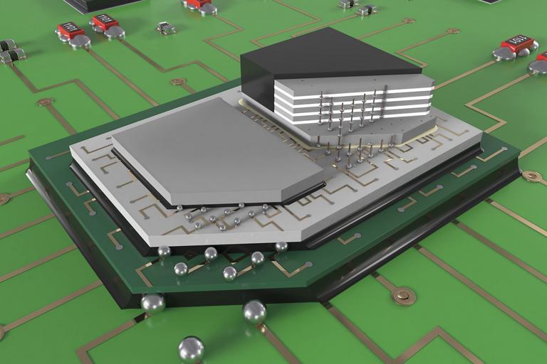
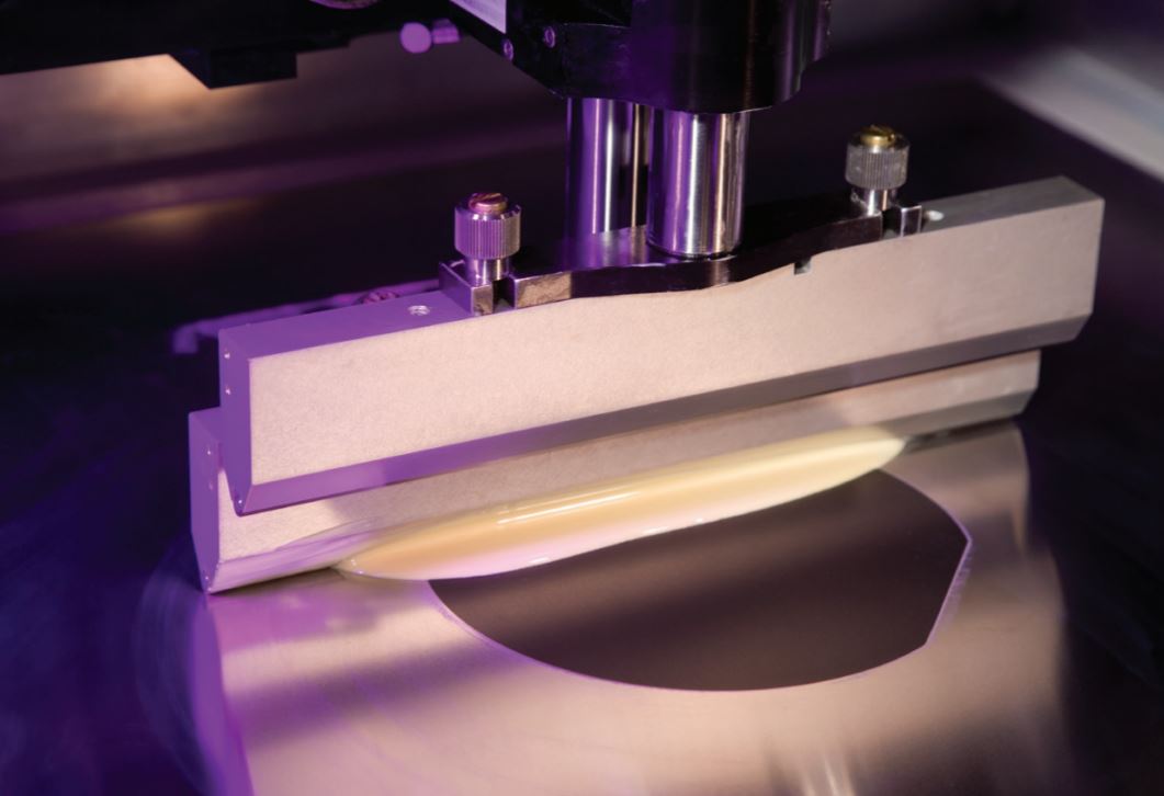
Wafer Backside Coating materials allow for screen or stencil printing of the paste across the entire wafer in a single stroke, increasing throughput by eliminating the need to individually dispense dots of adhesive. After B-staging to create a film, Wafer Backside Coating provides consistent bond lines and small, controlled fillets, which are particularly effective for attaching small die in miniaturized packages and challenging structures like chip-on-lead, where the die pad is smaller than the die.
The coating can be applied on Copper, Silver, or PPF (Palladium pre-plated leadframes) and the result can be MSL L1 capable with thermal conductivity varying from 2.2 up to 11 (W/m·K).