
.png)
-
Home

-
Electronics Assembly
- Printed Circuit Board (PCB) Assembly
Printed Circuit Board (PCB) Assembly
Printed Circuit Boards (PCB)
The electrical and mechanical foundation of modern electronics
A printed circuit board (PCB) is a rigid or flexible laminated board with patterned copper conductors that route electrical signals, distribute power, and mechanically support electronic components.
Anatomy of Printed Circuit Boards
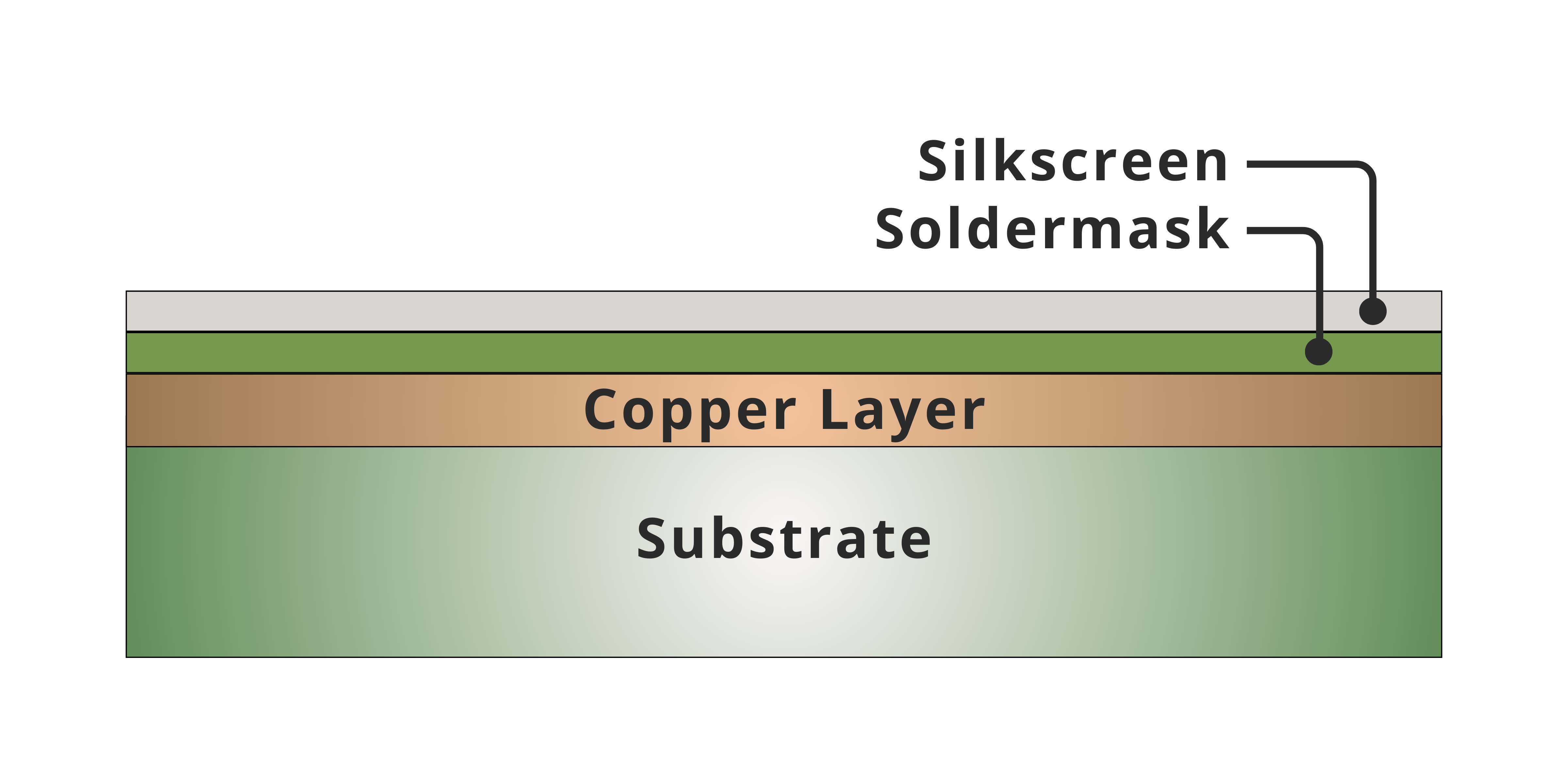
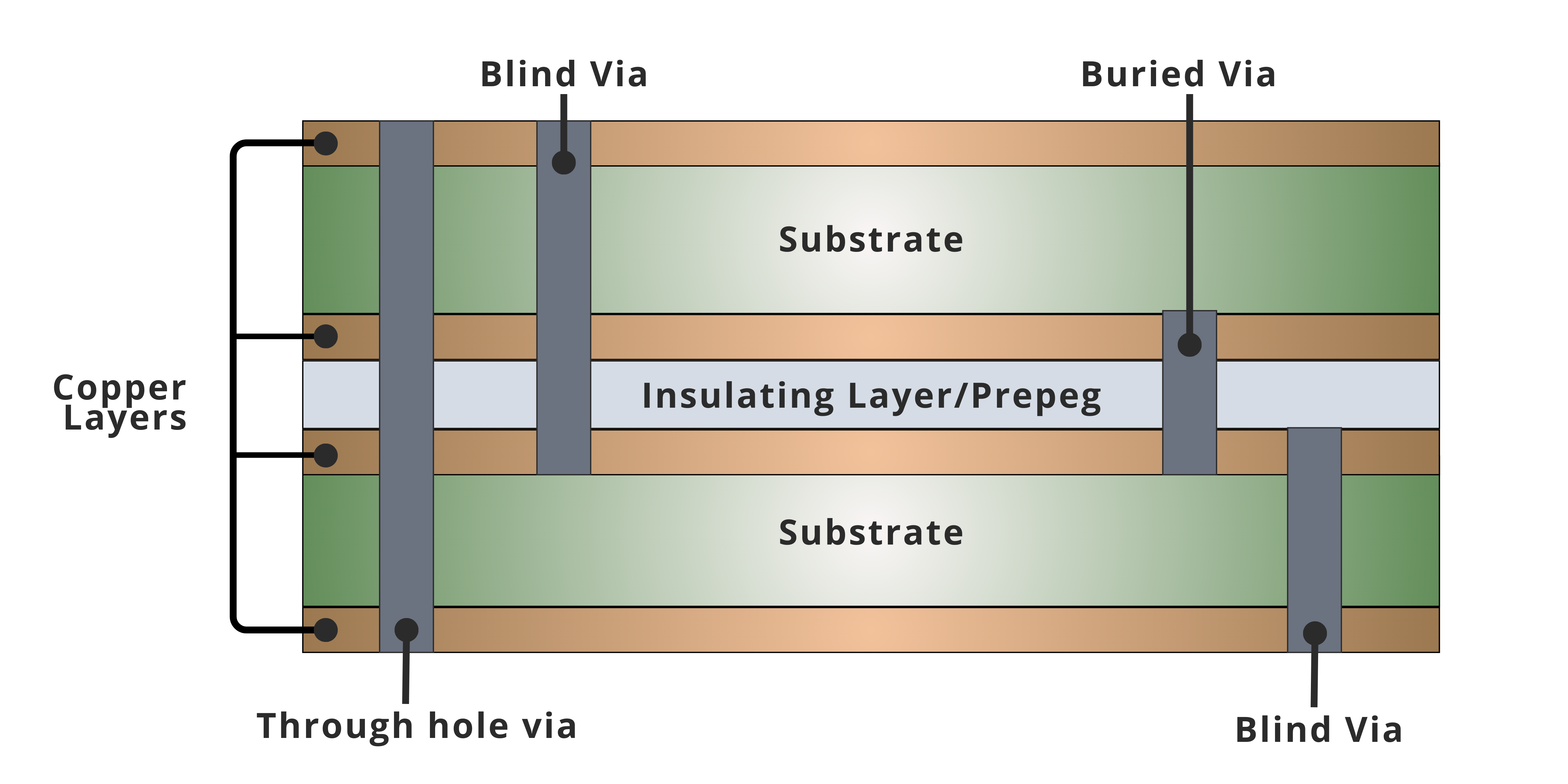
Distinct material layers providing mechanical support, electrical connectivity, and component identification
PCBs are composed of distinct layers, with single-layer PCBs using a simpler structure and multi-layer PCBs adding internal layers and vias to support higher circuit density and performance requirements.
PCB Market by Application (2020–2025)
Baseline PCB market value.
Post-pandemic recovery and demand rebound.
Mid-single-digit CAGR outlook.
Projected sustained growth rate.
Printed circuit boards form the electrical and mechanical foundation of modern electronics. Through copper traces, pads, and layered insulation, PCBs provide controlled signal routing, power distribution, and structural support for mounted components — enabling reliable integration of processors, memory, sensors, and power electronics into compact, high-performance systems.
Because of their central role, PCBs are used across consumer electronics, industrial equipment, automotive systems, and communication infrastructure. Market growth is therefore closely tied to trends in device complexity, electrification, connectivity, and automation rather than unit volume alone.
PCB Demand Concentrated Across Four Core End Markets
The largest share of global PCB demand, driven by smartphones, wearables, TVs, and IoT devices. High-layer-count and HDI boards dominate as device density and functionality increase.
Automation, controls, medical devices, and appliances. After contracting in 2020, demand has recovered alongside factory modernization and post-pandemic medical investment.
One of the fastest-growing segments, reaching approximately $10.6B in 2024. Fueled by EV power electronics, ADAS, infotainment, and vehicle connectivity.
Networking equipment, base stations, and wireless infrastructure. Expansion of 5G networks and data center connectivity continues to support this segment.
While PCBs provide the structural and electrical backbone of electronic systems, long-term performance depends heavily on PCB assembly materials. Adhesives, conformal coatings, thermal interface materials, and interconnect products determine how components are mounted, protected, cooled, and electrically connected throughout the service life of the assembly.
As PCB complexity and operating demands increase across consumer, industrial, automotive, and communication applications, material selection becomes a critical factor in ensuring durability, reliability, and compliance with evolving performance requirements.
Sources: Prismark Partners, Mordor Intelligence, Fortune Business Insights, TTM Technologies filings
PCB Assembly
From bare board to fully functional electronic assembly
Automated PCB assembly line illustrating stencil printing, component placement, and soldering
PCB Assembly Process Flow
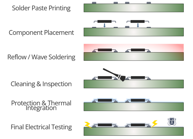
PCB assembly is the manufacturing process of mounting and electrically connecting electronic components onto a printed circuit board, transforming a bare PCB into a functional electronic assembly through a controlled sequence of material deposition, component placement, soldering, inspection, and testing.
It begins with board inspection and solder paste application, followed by automated component placement and thermal soldering. Cleaning, protection, and testing steps ensure electrical integrity, mechanical robustness, and long-term reliability.
Enables Precision & Repeatability
Automated stencil printing, pick-and-place, and reflow soldering deliver consistent placement accuracy, high throughput, and process repeatability in volume PCB manufacturing.
Supports Mixed-Component Designs
Modern PCB assemblies combine surface-mount, through-hole, and selective hand-soldered processes to meet electrical, mechanical, and thermal performance requirements.
Ensures Long-Term Field Performance
Cleaning, inspection (SPI/AOI), protective coatings, thermal interface materials, and final electrical testing are critical to ensuring durability and functional reliability.
PCB Assembly Materials & Technologies
Three material disciplines that govern every stage of the PCB assembly cycle
Transforming a bare PCB into a field-ready electronic assembly requires more than soldering. Each stage of the assembly process — from establishing electrical interconnections and protecting the board against its operating environment, to enabling reliable throughput on the production line — depends on a carefully selected set of specialty materials.
These materials divide into three functional disciplines. Interconnects create the electrical and mechanical bonds between components and the PCB — determining joint reliability, thermal cycling resistance, and compatibility with lead-free and high-density designs. Protection and reinforcement materials shield the completed assembly from moisture, chemical exposure, vibration, and mechanical shock throughout its service life. Supporting materials enable consistent, high-yield manufacturing by providing the process consumables, carriers, and substrates the assembly line depends on. Together, these three categories define the material stack behind every reliable PCB assembly.
Further Reading on Printed Circuit Board Assembly
Support Reliable PCB Assembly and Performance
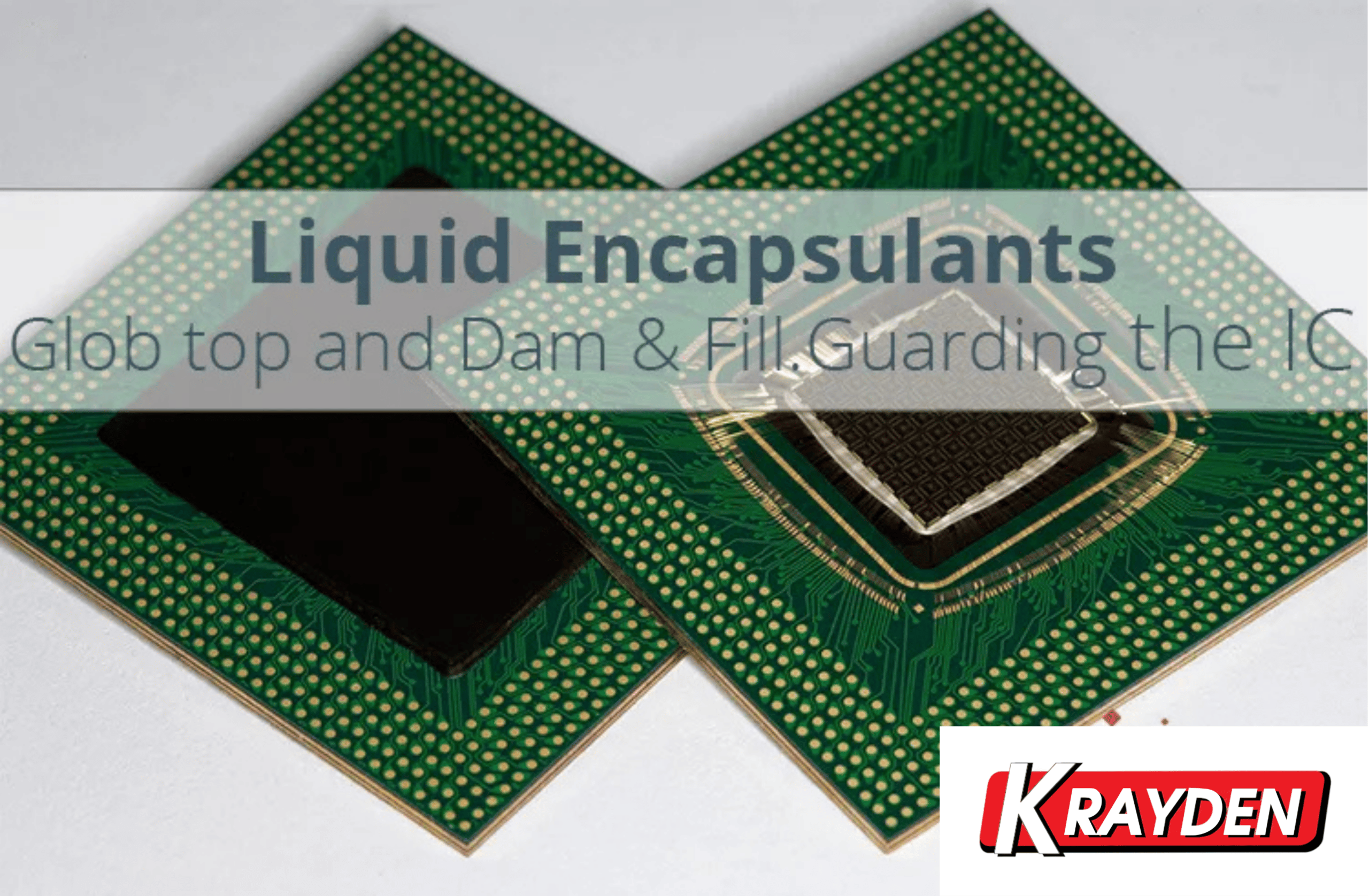
From thermal interface materials and structural adhesives to encapsulants and protective coatings, selecting the right materials is critical for PCB safety, reliability, and manufacturability. Contact us to discuss your application requirements, material compatibility, and system-level considerations.
PCB Assembly Materials – Quick Reference
.png)

