
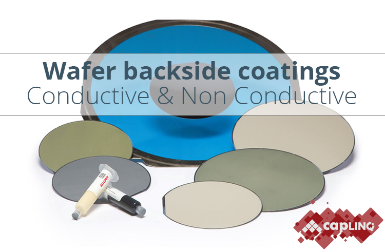
Die Attach adhesives, Films & Wafer backside coatings
Conductive and Non-conductive die attach films, pastes and wafer coatings
Die Attach Materials
Die attach materials are one of the most crucial parts of assembling microelectronics. From die attach pastes, to die attach films, solder pastes and wafer backside coatings, the options are almost limitless and picking the right material can literally make or break the final product. Whether it's connecting a semiconductor chip to a leadframe substrate, or connecting a semiconductor device to the designed circuit board, proper adhesion is critical.
To address the requirements for both laminate and leadframe wirebond packages, we provide a comprehensive portfolio of advanced die attach adhesives for various wirebond requirements – from smaller die-to-pad ratios to thinner bond lines to low stress to high temperature capability and robust adhesion. As a proud official distributor of the market share leader and top innovator of the most advanced die attach solutions, we offer Henkel’s LOCTITE ABLESTIK and ECCOBOND entire portfolio which delivers exceptional die packaging reliability performance and meets the highest JEDEC MSL standards.
There are numerous die attach adhesives available commercially. Proprietary chemical recipes are formulated to meet different application requirements or to address one persistent die attach challenge or the other. So how can you make a selection when you are faced with product inventory sheets a mile long of die attach variants? To help, we'll go through the common die attach adhesive categories and their relevant properties that will affect your selection.
CAPLINQ is proud to offer this complete range of die attach materials as seen in the subcategories below. Please continue to our Learn More section to, well, learn more about which die attach materials are available, the differences in their types and application methods, and how CAPLINQ can help you select and order the die attach adhesive that is right for your application.
Frequently Asked Questions
Frequently Asked Questions about Die Attach Materials & Die attach Adhesives
Why is Tg important when selecting the right die attach paste?
The glass transition temperature for organic adhesives is a temperature region where the polymers change from “glassy” to soft and rubbery. Increasing the temperature further continues the softening process as the viscosity drops too. Temperatures between the glass transition temperature and below the decomposition point of the adhesive are the best region for bonding. This window can span up to 100 degrees.
If Tg of the die attach is magnitudes lower than the wire bonding temperature, the die/chip could shift in the process, resulting in a weak bond. For thermoplastic adhesives, a too low Tg could result in the softening of the adhesive to the point that the die separates from the substrate at high enough temperatures.
Following these guidelines, we can avoid weak bonds and bleed out which typically happens at higher than necessary viscosities, caused by high temperatures.
Why is CTE important for die attach?
Using die attach pastes to bond substrates with different coefficients of thermal expansion (CTE) is a great challenge. Examples of difficult to bond combinations are ceramic to plastic, glass to plastic, and rubber to metal.
Here\'s what happens, temperature changes cause the different materials to expand according to their CTE leading to shear stresses and deformations after curing, or throughout the life of the device. The geometry of the design adds to the challenge.
The first point of approach is to select a die attach paste whose CTE is comparable to the CTE of both the die and substrate. Also, the die attach selected should contribute additional flexibility to the bond to compensate for the differences in material expansion. Thermoplastic adhesives are advantageous in this regard because of their characteristic low elastic modulus. They do not become brittle, unlike thermosetting adhesives.
Why doesn\'t Henkel list the MSL rating of all their products on their TDSs?
MSL performance is mostly determined by the package dimensions, e.g. die size, and other materials like lead frame and mold compounds used.
That’s why we can’t put this data on TDS. We do mention MSL performance in our technical data packages based on internal and external data availability.
Does the Tg of the material determine the maximum operating temperature of the device?
Tg is certainly giving some indication of its maximum operating temperature performance, but not always. Epoxy based materials with a Tg of 150°C for instance can have decomposition temperatures between 200 and 300°C.
The big advantage of high Tg die attach materials is the lower CTE mismatch with the Silicon die below Tg. On the other hand, BMI resin based materials like QMI 529HT with Tg of only 3°C have replaced a lot of high Tg epoxies when electronics assembly changed to Pb free 260°C reflow ~20 years ago. And the most temperature stable adhesives are Silicones with Tg far below 0°C.
Max is the maximum operating temperature of Die Attach Materials?
This depends on the temperature, the exposure time to the temperature and what you expect of the die attach material. During package assembly, die attach materials are exposed to a solder reflow, and in the case of lead-free solder, this temperature is 260°C, but the exposure time is less than 5 minutes. Operating temperatures tend to be far lower than these. "High Temperature Storage (HTS)" tests often run as high as 175°C for as long as 1000hrs. Manufacturers test that the device still performs after this test.
It is also important that you test the die attach materials yourself to make sure they meet your requirements, but generally you can assume that most die attach materials can operate up to 150°C continuously and 260°C intermittently for short durations. If you are looking for materials that have a continuous operating temperature above 175°C then you can contact us for product recommendations.
Learn More
Desirable Properties of Die Attach Adhesives
You'll need to compare your material properties, budget, manufacturing requirements, and other constraints to the properties and ease of using the die attach category that most closely qualify.
Properties That Depend on the Chemical and Physical Attributes of the Die Attach
- Thermal conductivity to dissipate heat generated in the device to heat sinks and other thermal management parts
- Electrical conductivity to efficiently manage and distribute electrical energy
- Excellent stability at the operating temperature
- Low modulus to eliminate warpage and reduce stress
- Negligible ionic contamination/good corrosion resistance
- Rapid bonding with good adhesion
- Negligible outgas interference
- Reliability when exposed to mechanical vibration and shock
Properties Associated with the Ease of Using the Die Attach During Product Manufacturing
- Curing cycle which impacts profitability depending on the scale of manufacturing, e.g., quick curing is more profitable for high volume manufacturing. Choose between in-line curing (snap) or off-line batch cure (oven, UV, etc.).
- Curing temperature that won’t affect parts.
- Storage conditions and pot life which dictate whether the adhesive needs to be stored frozen and how long after mixing/reaction it remains usable.
- Difference in coefficient of thermal expansion between die, die attach, and substrate. Small differences are preferable.
- Reworkability that makes it possible to decouple a die from its substrate, a useful property when expensive parts are used for testing.
- Compatibility with different-sized constructions, e.g., large dies vs. thin dies, intricate geometries.
- Die application, e.g., die stacking.
- Site preparation which affects throughput, e.g., cleaning and wetting procedures.
Challenges Associated with Die Attach Applications that Should Guide Your Selection
- Void formation: causes poor adhesion, poor heat transfer, and die tilting for die stacks. It also interferes with electrical performance.
- Bond line control: inconsistent bond thickness could lead to cracks and fractures as a result of different rates of thermal expansion and contraction of the die and adhesive. It can also affect the quality of wire bonding in semiconductor packages.
- Bleed out: When adhesive seeps out of the bond, it can contaminate the die surface.
Many die attach formulations might satisfy several of the parameters that matter to you. CAPLINQ can help you decide on the best die attach adhesive for your unique application, contact us today or learn more below.
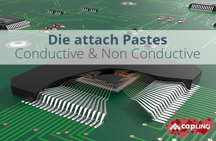
Conductive Die Attach Pastes
Conductive die attach pastes find the most significant application, about 80% of the die attach market, in attaching chips to leadframes where their electrical conductivity is an important parameter. These pastes are made of organic resins mixed with inorganic fillers. The resins could be thermosetting such as epoxy, phenolics, cyanate esters, and silicone or thermoplastics such as polyimides, and polyurethanes. Metal fillers such as silver, copper, gold, nickel, palladium have been used.
The resin is responsible for the mechanical properties of the adhesive, and the fillers are responsible for its electrical and thermal conductivity. Conductive die attach pastes form electrical connections between leadframes, I/O leads, active and passive devices, and other circuit components. They also act as channels that facilitate electrostatic dissipation and electrical grounding.
Based on their electrical conductivity, conductive die attach pastes can be classified as:
- Isotropic conductive adhesives (ICAs), popular for surface mount technology. They conduct electricity in all directions equally.
- Anisotropic conductive adhesives (ACA) used for adhering IC chips to glass panels in LCDs and in tape automated bonding packages. They conduct electricity in the Z-axis only.
- Non-conductive adhesives (NCAs) are useful in applications where the mechanical bond from the die attach is more important than its electrical conductivity.
A consequence of chips and devices becoming smaller is that they are susceptible to high temperatures experienced during electrical transmission. Without sufficient heat dissipation from a die attach material to appropriate heat sinks in a circuit, destruction and failure of parts become inevitable. Thermal conductivity is, therefore, a critical parameter affecting performance. For a paste to qualify as electrically conductive, its minimum thermal conductivity as specified by Method 5011 of the MILD-STD-883 standard is 1.5 W/m·K.
Properties of Conductive Die Attach Pastes Affecting Their Performance
Numerous conductive die attach pastes are available in the market, each with its unique differentiating property. The essential properties to consider that have far-reaching effects on the performance of any given product are: filler composition, morphology, manufacturing, and processing requirements.
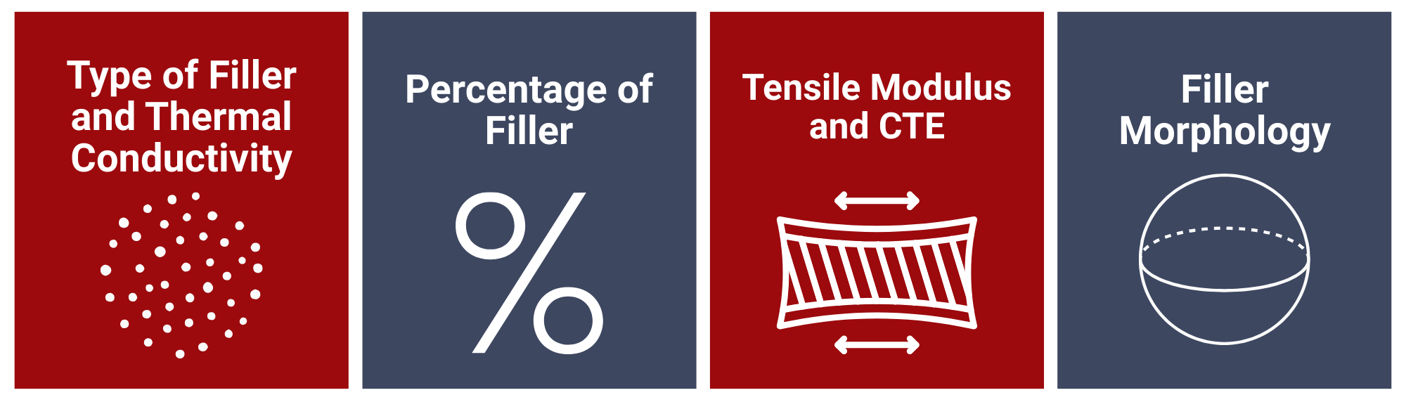
Type of Filler and Thermal Conductivity
The majority of polymer resin used in formulating conductive die attach are insulators by nature, so fillers are incorporated to increase their electrical and thermal conductivity. Fillers that have been used commercially are silver (429 W/m·K), copper (401 W/m·K), gold (318 W/m·K), and nickel (90-92 W/m·K). Their thermal conductivity values indicate why silver is so popular.
Understandably, silver-filled die attach pastes are expensive. However, silver exhibits other superior qualities including the fact that silver oxide is stable and conductive. On the other hand, copper-filled variants experience a decrease in conductivity with oxide growth after exposure to high temperatures. Nickel has a low oxidation rate, and given its lower thermal conductivity value, is a preferred filler in low-cost anisotropic adhesives.
Even though the thermal conductivity values of the filler metals are substantial, those of the formulated pastes are considerably lower. A value such as 1.9 W/m·K is not unusual for commercially available silver-filled pastes, while others as high as 7-11 W/m·K are also available.
Percentage of Filler
The filler percentage of a composite mixture is important because of the underlying trade-offs. A large amount of metal is necessary for greater conduction, but this affects physical properties like elasticity and mechanical strength.
According to percolation theory, a critical filler concentration exists where the 3-D network structure is established, and the increase in conductivity becomes significant by several orders of magnitude. Beyond this concentration, conductivity does not increase as noticeably with an increase in filler composition. Therefore, only a minimum quantity of filler is required to achieve a degree of electrical performance that is inherent to the composite. Typical values for ICAs lie between 25-30 vol % and 5-10 vol % for ACAs.
Filler Morphology
The characteristics of the filler material such as size, shape, orientation, and distribution in the mixture affect the viscosity/rheology of the formulation. These properties come into play in the bond line thickness. Since thin bond lines enhance thermal conductivity, fine particle sizes are preferable and it’s why metal powders with diameter sizes between 5-20 µm are typical.
Tensile Modulus and CTE
More than connecting materials together, adhesives act as load distributors. Assembled packages having different CTEs need a low modulus adhesive to compensate for the mismatch. Increasing the filler loading for the sake of high conductivity increases the tensile modulus of a die attach paste but decreases the ultimate strength. This could result in cracking during thermal cycling or vibration. Manufacturers use plasticizers to lower the modulus and add flexibility.
Processing Requirements
Parameters like temperature, cure time, pressure, storage conditions, and shelf life, impact not only the strength and reliability of a die bond, but also design and manufacturing decisions.
1. Manufacturing
In addition to the resin and filler, other components like hardeners, thinners and curing agents are added to modify cure rates, viscosity, and other mixtures properties. The die attach paste can be supplied as a single component where the catalyst is latent (usually by storing below -40°C ) until exposed to the given cure temperature. Supplied as two components, you get a separate resin, called part A, and the catalyst, part B. Either or both part A and B may contain the metal filler. The parts are weighed, mixed, degassed and cured. Cost-cutting objectives favor formulations that are solvent-free and have shorter cure cycles.
2. Curing
Curing involves the polymerization of the resins to solidify them into strong adhesive joints. Curing agents and sufficient heat (oven, UV) are often required for the reaction to occur and the type of catalyst will influence the cure time and temperature.
Typical pastes cure anywhere between 80°C to 180°C and some two-component die attach can cure at room temperature. Snap cure (often one-component) pastes derived from modified cyanate esters can cure in under 1-2 minutes making them an excellent choice for high volume manufacturing.
3. Storage
One-component formulations often need to be stored in a freezer, and this reduces the ease of using it. If stored incorrectly, adhesives can polymerize prematurely, absorb moisture, or crystallize. Also, if left too long before dispensing at room temperature, an adhesive mixture can separate leading to die bond inconsistencies where some parts are resin-rich and will flow excessively, while other parts are filler-rich and don’t flow easily. Die attach formulations based on bismaleimide resins were developed to counteract the tendency to absorb moisture.
4. Dispensing
Conductive (and non-conductive) die attach pastes may be syringe dispensed or stencil printed depending on the viscosity of the mixture.
Applications of Conductive Die Attach Pastes
- Leadframe packaging for suitable attachment to surfaces like copper, gold, silver, palladium, PPF
- Wirebond IC packaging for BGAs, PBGAs
- Printable chip on board devices, flexible circuit boards
Non-Conductive Die Attach Paste
Except for the difference in their composition and application, non-conductive die attach pastes are not far off from their conductive cousins. They are made of organic resins like epoxy, polyimides, silicones, acrylates and non-conductive fillers that could be metal, metal oxides, metal nitrides and more. Examples of ceramic and inorganic fillers are silica (SiO2), alumina (Al2O3), and beryllium oxide (BeO). An organic filler like PTFE has also been used successfully.
These pastes find the most use in die attach for semiconductors and surface mount devices, where a strong adhesion that can withstand physical and thermal stresses combined with strong electrical insulation is the priority. Example applications are automotives, sensors, consumer electronics, memory cards, RFID cards, USBs and LEDs.
There are applications where pastes with low thermal and electrical conductivity are sufficient. There are other situations, however, where pastes need high thermal conductivity because temperature control is critical. This second category are thermally conductive and electrically insulating die attach pastes. Unfilled polymer resins are natural thermal insulators (0.1–0.5 W/m·K), and the added fillers increase thermal conductivity tenfold or better. Method 5011 of MIL-STD-883 standard specifies the minimum thermal conductivity for electrically insulative die attach as 0.15 W/m·K.
Properties of Non-Conductive Die Attach Pastes Affecting Their Performance
.png)
Thermal Conductivity and Heat Dissipation
The thermal conductivity of silver-filled die attach pastes makes it excellent for heat dissipation, but in electronic applications where a high thermal conductivity must be combined with low electrical conductivity, ceramic fillers such as alumina and silica are good alternatives. Examples are packaging materials for power semiconductor devices where the heat generated needs to be dissipated to ensure its long life and reliability.
Thermal dissipation through the die attach occurs mainly through conduction and convection. Therefore, the morphology of the filler materials, their shapes, sizes and their distribution in the resin influence the process. Smooth ceramic powders less than 20 µm in diameter are typical.
Thermal Conductivity and Type of Non-Conductive Filler
The thermal conductivity of diamond is impressive, as high as 1500-2000 W/m·K depending on its purity, and that of diamond-filled pastes can exceed 12 W/m·K. However, the price of diamond is prohibitive for everyday applications. Fillers that have found commercial use are alumina (99%, 40 W/m·K), aluminum nitride (170-260 W/m·K), boron nitride (130-260 W/m·K), and silicon carbide (270 W/m·K).
Percentage of Filler and Flow Properties
Boron nitride at a loading level of 40 wt% can produce a mixture with a bulk thermal conductivity of 8-10 W/m·K, although the thixotropic end result can be difficult to dispense. On the other hand, alumina is low cost and a popular choice due to its more manageable flow properties. When mixed with organic resin, the resulting paste has a thermal conductivity of 1.5 W/m·K at a loading level of 75 wt%.
Therefore, although the thermal conductivity of a paste may be increased by adding more filler as far as the density of the resin will allow (typically, 85%–90% by weight and 40%–50% by volume), there is a point where doing so is no longer beneficial, negatively impacting other properties of the paste, e.g., viscosity. To counter this, thixotropic additives are introduced to improve flow properties. You will find that many commercially available die attach pastes are formulated using similar core resins, fillers, and catalysts but differ in the quantities of these ingredients.
Another factor affecting the thermal conductivity of a paste other than type and percentage of filler is the curing requirement of the paste.
Electrical Insulation
Non-conductive die attach pastes are required when it’s essential to inhibit the flow of electricity (avoid electrical interference/ isolate electric current). In order to understand how non-conductive die attach pastes compare in fulfilling these needs and requirements, it will be helpful to define a few parameters you will come across in data sheets:
1. Dielectric constant: a dimensionless ratio that measures the ability of a material to store electrical energy when exposed to an electric field. The dielectric constant for non-conductive die attach pastes used for electrical insulation will typically lie between 2-5. A higher value in the range 6-12 is acceptable where some electrical conductivity can be overlooked.
2. Dissipation factor: measures the power loss in a material experiencing an alternating electric field, a ratio of the power dissipated to the power applied. A low value implies the die attach paste, the substrates to which it adheres, and the surrounding circuit components will experience only low levels of heating. At ambient temperatures, typical DF values lie between 0.003 to 0.030 at 1 KHz, and can go up to 0.050 at 1 MHz.
3. Dielectric strength: measures the maximum voltage that, when applied across a material, won’t cause dielectric breakdown. Beyond this point (breakdown voltage), a non-conductive die attach paste becomes electrically conductive. Also, dielectric strength decreases as temperature or frequency increases.
Mechanical Strength and Coefficient of Thermal Expansion
The resin part of the paste is responsible for providing shear and tensile strength to the adhesion throughout all the possible conditions an assembly will encounter. Apart from thermal conductivity and flow properties, the type of filler used influences the CTE of the paste which is critical when bonding dissimilar materials together. Unfortunately, while these fillers may improve the CTE, their addition negatively impacts the bond strength. It becomes a trade-off decision about what the percentage of filler loading should be for an application.
Processing and Dispensing
Non-conductive pastes may be based on thermoset or thermoplastic resins. The paste can be supplied as a single component with a latent catalyst/ hardener or a two-component mixture, requiring expert weighing, mixing and degassing of the resulting composite.
Die attach pastes (conductive and non-conductive) can be deposited into any shape through syringe dispensing or stencil printing, making them ideal, where the components to be bonded, have interesting geometries. They can also be scaled for mass manufacturing and automation using high-end equipment that is optimized for all the critical parameters to avoid common defects such as voiding and bond thickness variation.
Application
- Leadframe packaging for proper attachment to surfaces like copper, gold, silver, palladium, PPF
- Laminate packaging in BGAs, LGAs
- Printable board on chip for DRAM devices, flexible circuit boards
- For bonding high power LEDs and surface mounted devices, SMDs to PCBs
- For bonding ICs to heat sinks
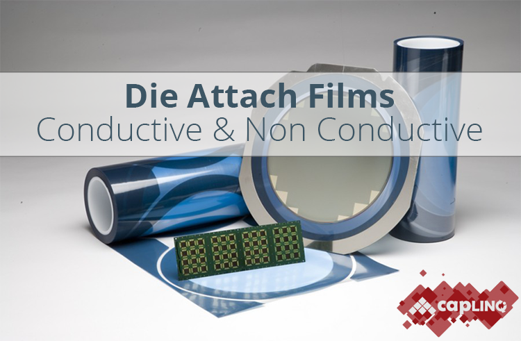
Conductive Die Attach Film (DAF)
Conventional die attach pastes are still plagued by inconsistencies that lead to voids, bleeds and uneven bondlines in assembled packages. This unreliability is an issue because the demand for smaller-sized semiconductor packages with increased functionality, like those used in many handheld electronics, keeps growing.
Small-sized packaging calls for reduced footprint on a printed circuit board. This is accomplished by assembling multiple dies in the same package. When die attach pastes are used for die stacks, especially with difficult die-to-pad ratios, the challenges mentioned above can result in low yields.
Die attach films were created to solve the inconsistency issue in multichip modules and other applications involving wafer-level and die size limitations (e.g., thin dies <100µm). In general, any situation where the problem of too little, or too much die paste can give rise to resin spreading (contaminating the die), large fillet formation (problematic for close die configurations), and resin overflow (causing poor wire bonding), films are the preferred solution.
Composition of Conductive Die Attach Film
Looking at their core ingredients, conductive die attach films are fundamentally similar to paste versions. They are made from organic resin that may be thermoplastic or thermosetting, incorporated with a conductive filler, and dried into sheets/film of thickness ranging anywhere between 10-40 µm.
Polymer resins like epoxies, maleimides, bismaleimides, acrylates, silicone, cyanate esters have been used successfully in commercial films. And conductive fillers like gold, copper, silver, and nickel widely used.
Conductive die attach films are used as adhesives for circuit substrates, and heat sinks joined to metal or ceramic packages and PWBs. Silver-filled films are popular because of their high thermal conductivity in the order of 6 W/m·K. The typical electrical conductivities that make a film useful for EMI shielding lie in the range 5 × 10⁻³ to 5 × 10⁻⁴ ohm-cm.
Preparation of DAF
In general, a pre-mixed composite similar to die attach paste is coated onto a release liner, and together they are laminated to a reinforcement/carrier such as PVC or glass fabric. This provides structural support during fabrication and handling. Alternatively, for wafer-level applications, the resin composite plus carrier are laminated with dicing tape to produce dicing die attach film. It streamlines manufacturing and makes automation feasible, where cut wafer pieces are easily picked and positioned.
Film makers ensure the DAF and dicing tape have good bonding, and at the same time, the tape can be released without leaving residue on the film. UV and thermal release films are popular for this reason. Conductive die attach film can be purchased as:
- Sheets or rolled sheets (e.g., 500 sheets per roll) that the user will cut into the desired shape to fit the die.
- Pre-cut sheets, sized for specific devices.
- Pre-attached to leadframes and substrates for extra convenience.
Properties That Can Affect Conductive Die Attach Film Selection

Die Mounting Temperature
Supplier recommendations for bonding temperatures are a good place to start. The stipulated temperatures show the strongest bonding strength for specified materials. However, because the surfaces to be bonded can vary (roughness, type of material and level of contamination), the die attach process will need to be tested for each new product before scaling production.
Therefore, optimization is necessary to determine the bonding force, temperature, and bonding time that will achieve the strongest bond possible with minimum bondline thickness and negligible voids.
Tg, Viscosity, and Low Stress
The stress characteristics of packages with film adhesives are a function of CTE, elastic modulus, and Tg to varying degrees.
Low modulus DAF can absorb a large amount of stress before fracture occurs. However, because the modulus for thin films at high temperatures is difficult to determine, adhesion at high temperatures is an important parameter when selecting a DAF variant. A DAF with high Tg is recommended at high temperatures. The Tg is the point (range) where the film changes from glassy solid to rubbery. As such, operating close to Tg means that the reliability of an assembly can become compromised. Testing the elastic modulus of a DAF at different temperatures is important.
Dicing
Optimizing the dicing parameters ensures dicing occurs with minimal chipping, cracking, or flying die. Die fly when the adhesion between DAF and dicing tape isn't strong enough. On the other hand, too strong an adhesion will lead to difficulties for die pick up. Appropriate film selection makes a trade-off between these competing challenges.
Good Wetting
For handling thin wafers and large die sizes, films characterized with excellent wetting are recommended to enable complete and robust adhesion to substrates. This removes the need to apply excessive pressure that may damage the wafer. On the other hand, poor adhesion in large die can lead to warping and other problems.
Compatibility
For wafers, a film that is compatible with the various wafer processing stages will add a higher level of flexibility and performance to the manufacturing process. For other applications, the type of resin a film is composed of should agree with the substrate, whether metal, glass, ceramics or organics and also the end-use device. The manufacturer\'s guidelines will prove useful here.
Curing
With every application of heat, the film gets partly cured. This is not a significant issue for processes with few heating steps. However, for multichip packages, the total heat applied for heat treatment at wafer lamination, die attach and wire bonding needs to take into account the curing required for molding. There\'s a risk of delamination when attempting to mold packaging with fully cured DAF.
Certain films need heat and pressure to be applied simultaneously during curing, e.g., anisotropic films (so that metal filler particles become aligned) or where plastic substrates are involved (so that trapped air and volatiles can be pushed out). Techniques for preventing trapped air or moisture bubbles include curing under vacuum and vacuum baking surfaces before adhesion.
Storage
DAF contains UV-sensitive components. Therefore, exposure to ambient light for periods of time can initiate curing. Rolled film can be stored from 6 months to a year (depending on the manufacturer) in a dark place before it loses its effectiveness.
Ideally, based on their storage time and minimum order quantity, DAF is suited to large scale manufacturing where these requirements will be matched by production volume to prevent wastage.
Applications
- Board on chip
- Leadframe semiconductor packages: QFNs, TSOPs
- Wirebond laminate packaging: Logic IC, RF, and MOSFET
Non-Conductive Die Attach Film
The first die attach films to be manufactured were non-conductive. Moreover, their prices are not as prohibitive as conductive variants. Non-conductive films are useful for many of the same reasons: for preventing adhesive bleeding, voiding, and inconsistencies with bond line thickness.
They are required wherever multiple bare chips are to be stacked on top of one another since smaller package sizes help improve signal integrity and thermal path in modern packaging technology. Examples are 2.5D and 3D-TSV system in package (SIP) applications for high-end memory storage.
Composition of Non-Conductive Die Attach Film(NCF)
Non-conductive die attach films are made from either thermoplastic or thermosetting polymer resin that is incorporated with a non-conductive filler. The composite is coated on a liner, and laminated on a carrier (for support) using pressure and heat.
Organic resins like epoxies, polyimides, bismaleimides, acrylates, silicone, cyanate esters and non-conductive fillers like silica, alumina, aluminum hydroxide, mica, glass, and organic fillers like PET have been used in manufacturing NCF.
These films are electrically insulating to ensure the electrical integrity of circuits. They are used for maintaining the physical connection between the electrode pads and bumps in chip on board (COB) and chip on glass (COG) applications, and for safeguarding fine pitch devices.
Their thermal conductivity (1.5–1.6 W/m·K) comes into play for bonding heat-dissipating components to heat sinks. As such, diodes, transistors, resistors, and thermal-sensitive integrated circuits can be mounted reliably to PCBs.
Manufacturers have also combined NCF and dicing tape into a single product for adding flexibility to automated wafer processing and assembling.
Advantages of Non-Conductive Die Attach Films
The Importance of No Fillet in Thin, Small Die and Multiple Die Packaging
In traditional die attach paste applications, the leadframe pad is larger than the die. The applied paste flows and forms a fillet around the die edge but must not spread past and flow to the top surface of the die.
Die attach films make the dispensing step obsolete. In most cases, thermal compression bonding melts the film between a die and its substrate. As a result of negligible fillet formation or bleeding, die attach films are suitable for configurations demanding tighter clearance between die and die pad, making it possible to incorporate more die per package, such as in LGA and PBGA. In comparison, using pastes, larger die pad sizes means fewer dies per package are possible.
Processing and Manufacturing are Easier to Control
A wafer already backed by die attach film eliminates the need to apply paste to individual die, essentially removing a repetitive stage from the manufacturing process. Also, no second guessing the thickness of the applied adhesive is required. The film thickness decides the width of bondlines.
The drawbacks of film are their higher price, the need for additional equipment, and generally, their lower thermal and electrical conductivity compared to paste variants. However, manufacturers are still coming up with films having higher thermal conductivities than their previous film products.
Die Sizes
Initially developed for devices using die sizes less than 3x3mm, film manufacturers continue to push the boundaries so their products are suitable for a wider range of die sizes. You will find that often, suppliers offer different grades of dicing die attach film depending on the size of the die. For smaller die sizes (2x2mm), increased adhesion to the dicing tape is implemented to prevent die flying off during dicing. Die attach films for sizes less than 1x1mm and thickness less than 100 µm are now available commercially.
Properties That Can Affect Non-Conductive Die Attach Film Selection
Dielectric Strength and Dissipation Factor
To provide the required electrical insulation, a NCF will be characterized by low dielectric constant and low dissipation factor. Dielectric strength measures the likelihood of the film breaking down when exposed to a high enough voltage and becoming conductive as a result. Suppliers will state the maximum voltage a component featuring their NCF film can experience and still continue to operate normally.
A low dissipation factor indicates low power losses and the corresponding low heating of circuit components in close proximity.
Curing
Cure temperatures provided in supplier data sheets should achieve complete polymerization of the NCF and the strongest adhesive strength. At temperatures other than what is provided, poor wetting and severe reliability issues can result. Temperatures between 125-150°C for 1-2 s are common, although there are specialized formulations with lower cure temperatures and faster cure times which are attractive for multichip modules.
Voiding and CTE
Even though compared to paste variants, films exhibit low voiding, voids can become an issue when films are not applied properly (100% void-free is unlikely, 5% is acceptable in many applications).
A few factors that can contribute to voiding are the NCF\'s viscosity, thermal stability, chemical stability, the evenness of the adhering surfaces, and moisture absorption especially for plastic substrates (plastics have uneven surfaces and are hydrophilic). To overcome voids, users will need to address these factors, e.g., through pressure application, substrate preparation, filler selection, and so forth.
The mismatch of the CTE of different packaging materials is often the direct cause of warpage that leads to cracking. Used as an adhesive, the selected NCF should be lower than the CTE values of the die and substrate to minimize mechanical stresses after bonding. The presence of voids combined with thermal expansion can lead to film failure.
Storage
After UV exposure, some film variants deteriorate to such a level that the die pick up and place process is compromised. And due to their expense, it’s important to take into account the work-life of stored NCF.
Suitability to Processing and Compatibility to Various Substrates
Wafers laminated with NCF will still need to undergo further processing conditions without degrading in adhesive and mechanical strength, or thermal properties, e.g., stealth dicing before grind (SDBG) process.
Also, the selected film should exhibit excellent wetting and compatibility with typical substrates and applications, e.g., Cu and Au wire packages, solder masks, etc.
Application
- Board on chip
- Leadframe semiconductor packages: QFN, QFP, SOIC, TSOP, and TSSOP
- Wirebond laminate packaging: memory, sensors, Logic, MEMS
Selecting the Best Conductive Die Attach Paste for Your Unique Application
Numerous die attach formulations are available, up to the thousands, and they differ widely in properties. Let us know the unique requirements of your product or process, and we can help pinpoint the best adhesives for your needs. CAPLINQ offers a variety of die attach adhesives for numerous applications:
- Laminate and leadframe packaging,
- Semiconductors: QFN/QFP, SOP/DIP, LGA, BGA,
- LED packages, and
- Discrete electronic components: capacitors, inductors, transistors
| Term | Description |
|---|---|
| BGA | Ball Grid Array |
| BMI | Bismaleimide Resin |
| CBGA | Ceramic Ball Grid Array |
| COB | Chip On Board |
| CSP | Chip Scale Package |
| CTE | Coefficient of Thermal Expansion |
| DIP | Dual In-Line Package |
| EMI | Electromagnetic Interference |
| FBGA | Fine Ball Grid Array |
| IC | Integrated Circuit |
| LGA | Land Grid Array |
| MEMS | Micro-Electro Mechanical Systems |
| MOSFET | Metal-Oxide Semiconductor Field-Effect Transistor |
| MSL | Moisture Sensitivity Level |
| PBGA | Plastic Ball Grid Array |
| PGA | Pin Gird Array |
| PPF | Pre-Plated Finishes consisting of layers of Ni, Pd and a Au finish |
| PTFE | PolyTetraFluoroEthylene |
| QFN | Quad Flat No-leads Package |
| QFP | Quad Flat Package |
| RF | Radio Frequency |
| SIP | System-in-package |
| SOIC | Small Outline Integrated Circuit |
| TSOP | Thin Small Outline Package |
| TSSOP | Thin-Shrink Small Outline Packages |
| Cure type | Description |
|---|---|
| B-stage | Partial cure until the material is in a solid state and relatively tack-free at room temperature, but will soften and flow when heated |
| Oven cure | Standard thermal cure in a traditional box oven, usually between 15 min. and 1 hr. |
| Snap cure | Fast thermal cure via in-line oven, with or without contact heat, usually under 2 min. |
| SkipCure | Very fast thermal cure that can be partially cured during the wirebonding process and fully cured during the molding process |
| UV cure | Cure by exposure to ultraviolet light |
Presentations
Die Attach Paste Developments
This presentation provides a comprehensive overview of die attach paste technologies, from fundamental concepts to the latest material advancements. It covers the role of die attach materials in semiconductor packaging, key performance requirements, and the evolution of adhesive formulations designed to meet increasing demands for thermal management, electrical performance, reliability, and miniaturization. Attendees will gain insight into both traditional and advanced die attach solutions used in modern microelectronics applications.