
Reliability testing
Material, Stress, Mechanical and Environmental induced mechanisms
- Home

- Semiconductors
- Reliability
- Common Reliability Tests
Common Reliability Tests
Temperature Cycling Test (TCT)
During the temperature cycling test (TCT), semiconductor packages are exposed to extremely low and extremely high temperatures commonly for 1000 cycles. Therefore, TCT measures the ability of semiconductor packages to withstand mechanical failure due to cyclic exposure to thermal effects.
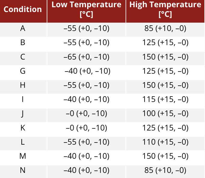
TCT Conditions according to JEDEC JESD22-A104
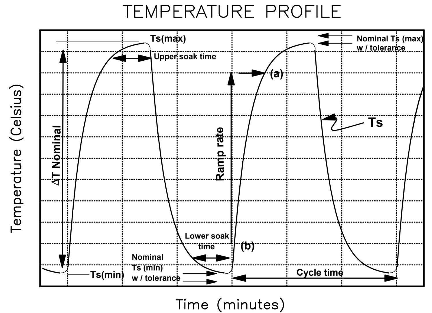
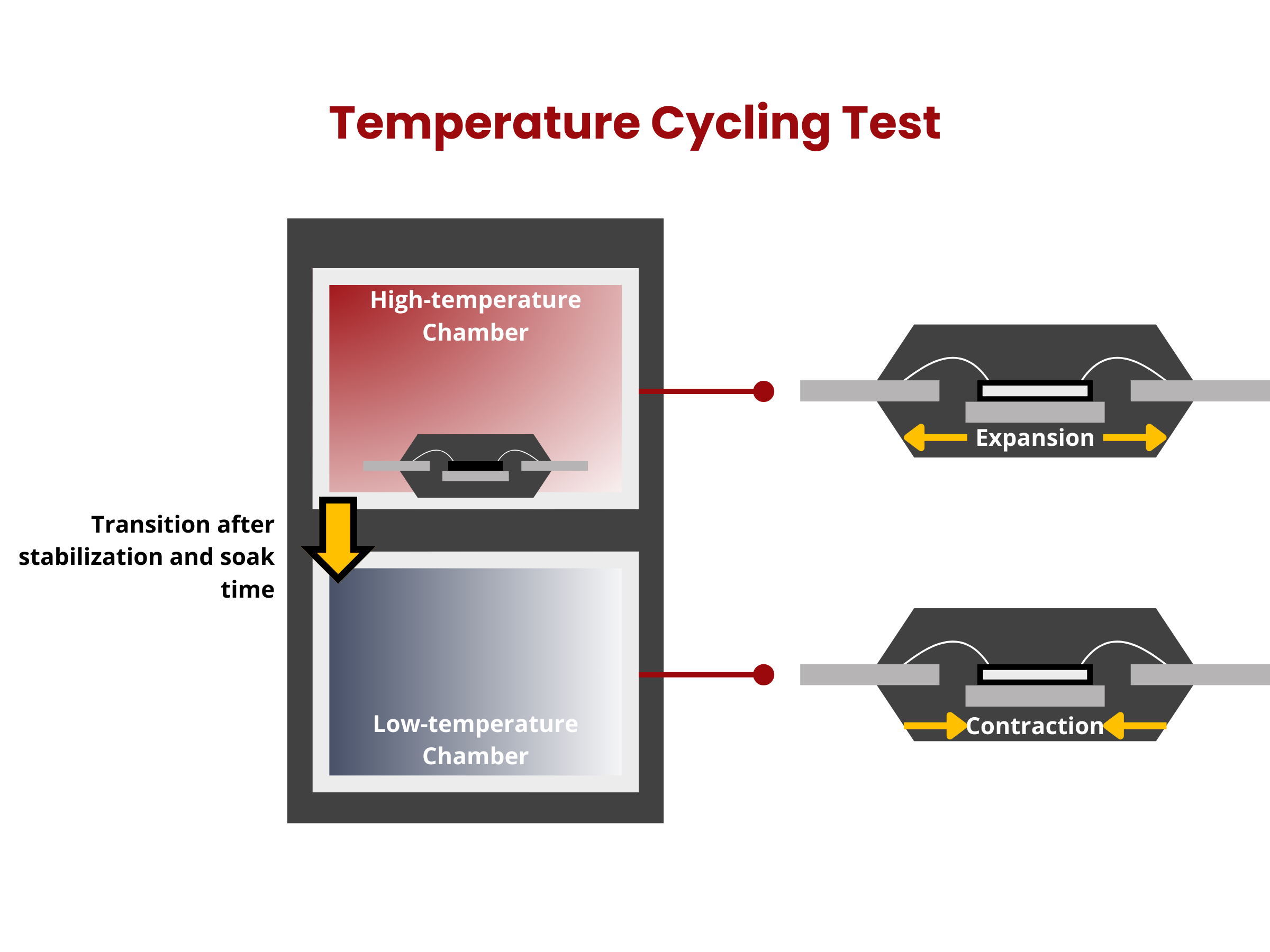
TCT is performed in a chamber wherein the semiconductor package is held at high and low temperatures. Typically, the sample is held at one extreme temperature setting after stabilization for a certain period of time, which is commonly referred to as the soak time. After the intended soak time, the sample is transitioned to the other temperature setting. The number of test cycles and soak time are often varied to trigger different failure mechanisms in the packages or parts being evaluated.
 Source: JESD22-A104C Standard for Temperature Cycling
What happens during TCT?
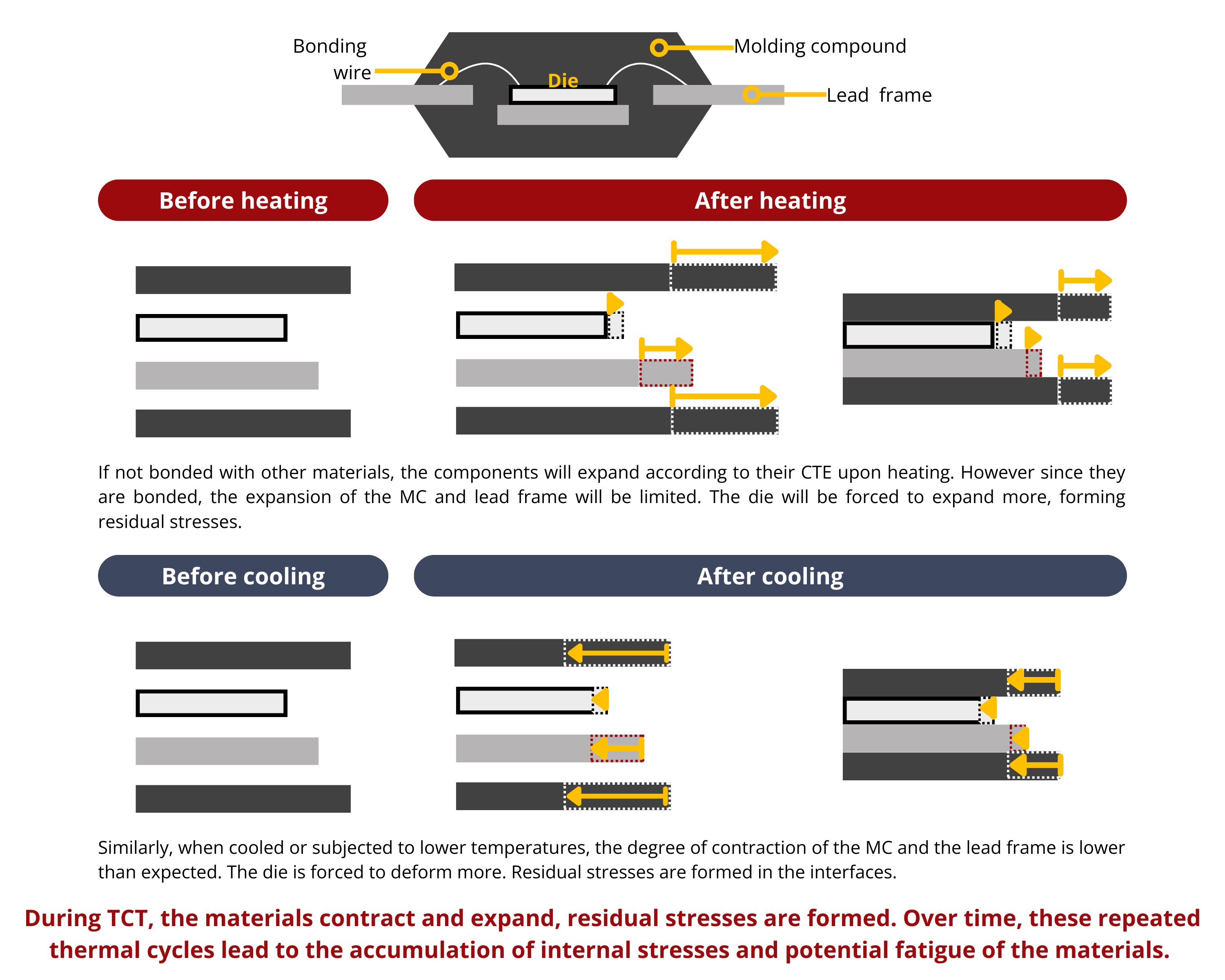
During thermal cycling, the semiconductor die, the metal lead frame or organic substrates, and the organic molding compound will contract at different extents. Most likely, the plastic molding compound and metal lead frame would want to expand more than the die. However, since they are attached, the degree of expansion will be less than that of what is expected. This, therefore, exerts a compressive force on the mold compound or the lead frame. Conversely, the die that has very low CTE is forced to expand beyond the expectation because the other components pull it. This puts a tensile (pulling) stress to the die. This phenomenon yields residual stresses on all the interface, which could lead to device failure. At high temperatures, the package components expand. At low temperatures, they contract. Over time, these repeated thermal cycles during TCT can lead to the accumulation of internal stresses and potential fatigue of the materials. This can eventually lead to device failure, which is a critical concern, especially for semiconductor devices used in applications where reliability is paramount.
Typical Failure Modes observed during TCT
- Delamination between interfaces
The repeated expansion and contraction of materials can lead to the accumulation of residual stresses, which can weaken the adhesion between layers over time and consequently lead to delamination. - Die cracking
Cracks may form within the semiconductor die itself due to the stresses it experienced during TCT. - Metal layer displacement
The stress generated during temperature cycling can cause the chip metallization to move or deform. These movements might not be visible to the naked eye, but they can be significant at the microscale. Over time, these movements can potentially lead to the metal layers shifting out of their intended positions or causing microscopic cracks and defects.
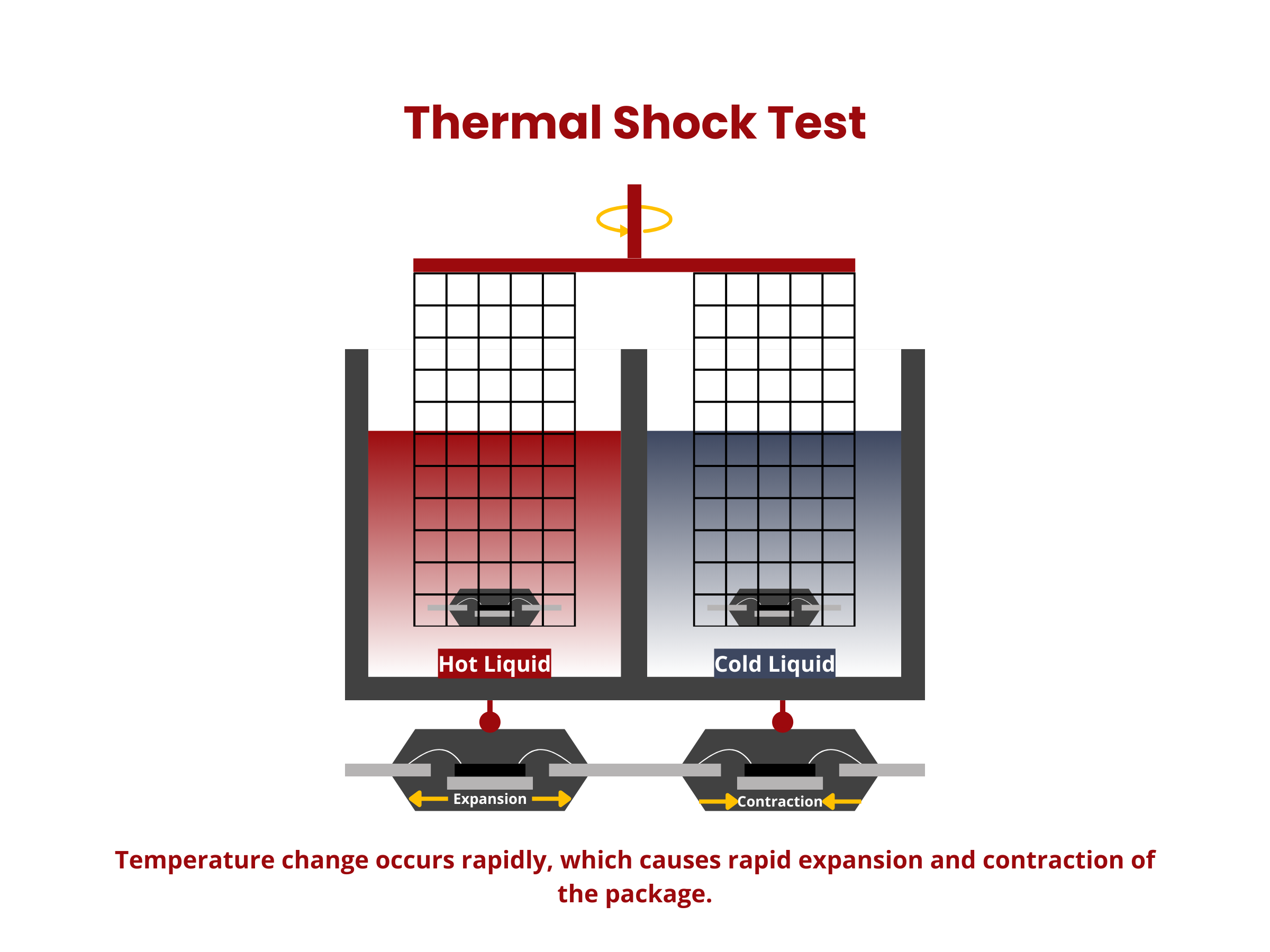
Thermal Shock
Similar to TCT, thermal shock is an accelerated test performed to elicit different failure modes in semiconductor packages by exposing them to temperature changes. The difference, however, is that during thermal shock, the temperature change occurs rapidly, i.e, the stabilization period and soak time are relatively short. Rapid temperature changes tend to mimic thermal effects during the self-heating of high power devices, turning on and off of optical devices, and wave soldering. This testing is also performed in chambers, which often contain liquids held at two extreme temperatures. Compared to that in TCT, which is conducted in air chambers, heat transfer and absorption using liquid media are more efficient, making thermal shock as one of the most severe temperature-related reliability tests.
Thermal Cycling vs. Thermal Shock Tests
| Characteristic | Thermal Cycling Test | Thermal Shock Test |
|---|---|---|
| Purpose | To evaluate a material or component's response to repeated temperature fluctuations. | To assess how a material or component withstands rapid temperature changes. |
| Testing Method | Gradual temperature changes over an extended period (hours, days, or even weeks). | Rapid temperature changes within seconds to minutes. |
| Stress Mechanism | Mechanical stress primarily due to thermal expansion and contraction over time. | Mechanical stress due to sudden thermal gradients, leading to rapid expansion and contraction. |
| Typical Application | Used to simulate real-world conditions where temperature variations occur gradually, such as in electronic devices or aerospace components. | Used to test materials or components that may experience rapid temperature changes, like automotive parts in cold climates or electronic devices subjected to extreme conditions. |
| Testing Frequency | Longer test durations with many cycles (thousands to millions). | Fewer cycles with rapid temperature changes (tens to hundreds). |
| Failure Detection | Detects gradual degradation over time, including fatigue and material wear. | Identifies immediate defects or weaknesses in the material or component that may result from sudden temperature changes. |
| Equipment | Requires a single chamber | May require multiple chambers to rapidly change the temperature |
| Standards | Compliance with standards such as MIL-STD-883 Method 1010 and JEDEC JESD22-A104 | Standards like MIL-STD-202 Method 107, MIL-STD-883 Method 1011, JEDEC JESD22-A106, and MIL-STD-750 Method 1056 |
Thermal shock temperature conditions and recommended fluids according to JEDEC JESD22-A106B
Place the test specimens in the bath in a manner that allows liquid to flow freely around and over them. Apply the specified conditions to the load for a set number of cycles. If necessary, interruptions can occur during the test due to loading/unloading device lots or equipment failures. However, should interruptions surpass 10 percent of the total specified cycles for a given test, it must be restarted from the beginning.
Failure criteria
After the test, visual examination and electrical tests should be performed. A device is considered a failure if it cannot demonstrate functionality under nominal and worst-case conditions. Mechanical damage, such as cracking, chipping, or breaking, is also considered failure, provided that these were not induced duting testing of handling.
| Test Conditions | A | B | C | D | |
| Step 1 | Temperature tolerance (°C) | 85 +10/-0 | 100 +10/-0 | 125 +10/-0 | 150 +10/-0 |
| Recommended fluid | Water or Perfluorocarbon | Perfluorocarbon | Perfluorocarbon | Perfluorocarbon | |
| Step 2 | Temperature tolerance (°C) | -40 +0/-10 | 0 +0/-10 | -55 +0/-10 | -65 +0/-10 |
| Recommended fluid | Perfluorocarbon | Perfluorocarbon | Perfluorocarbon | Perfluorocarbon | |
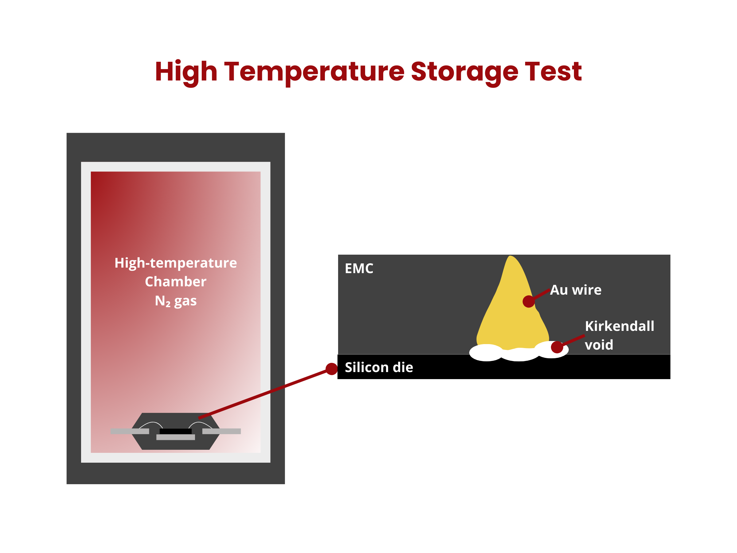
High Temperature Storage Test
High temperature storage test (HTST) is performed to evaluate the capacity of semiconductor packages to withstand exposure to high temperature for a prolonged period of time without any applied electrical stresses. HTST is effective in accelerating failure modes that are affected solely by temperature. Any chamber or equipment, such as convection ovens and bake chambers, capable of applying controlled high temperature may be used for this test.
High temperature storage conditions according to JEDEC JESD22-A103C
The packages under test shall be held at one of the following temperature conditions under continuous storage (at least 1000 hours).
| Condition A | +125 (-0/+10) °C |
| Condition B | +150 (-0/+10) °C |
| Condition C | +175 5-(0/+10) °C |
| Condition D | +200 (-0/+10) °C |
| Condition E | +250 (-0/+10) °C |
| Condition F | +300 (-0/+10) °C |
| Condition G | +85 (-0/+10) °C |
What happens during HTST?
Exposure to constant, high temperature triggers temperature-sensitive processes, such as oxidation and diffusion of chemical species. When held at a high temperature, epoxy molding compounds get oxidized, which may alter and degrade their mechanical properties. On the other hand, the diffusion of chemical species within the package forms Kirkendall voids. Void formation may be observed at different critical regions of the semiconductor package; however, the Kirkendall effect (void formation from temperature-induced diffusion) is more prevalent in the soldering materials.
Typical Failure Modes observed during HTST
- Solder joint failure
High temperature causes chemical species diffusion with the solder, forming voids and gaps between the solder–substrate interface. The degradation of the solder joints result to open failure (forms open circuits), which reduces electrical conductivity. - Oxidation and corrosion
EMCs undergo thermal aging (oxidation) at elevated temperatures. Oxide layers form on the EMCs and their thicknesses increase with increasing temperature. Oxidation drastically affects the mechanical properties of the EMC: it (1) increases the storage modulus, and (2) changes the glass transition temperature and coefficient of thermal expnasion, which can all affect package reliability. The metallic components within the package are also susceptible to corrosion during HTST. - Thermal cycling-induced stress
Thermal cycling at high temperatures can introduce mechanical stress, potentially causing delamination, cracks, or fatigue failure in package materials.
Temperature, humidity, and bias (THB) Test
Temperature, humidity, and bias test (THB) evaluates the reliability of electronic packages under humid environments. During THB, temperature and humidity drives the corrosion of the semiconductor components. Similarly, a voltage bias is applied across the device to mimic the bias conditions the device experiences in its actual operational environment, with the aim of maximizing the variations in potential levels among various metallization areas on the integrated circuit as much as feasible. THB is often performed at 85 °C and 85% RH, that is why it is called as the 85/85 test.
THB is performed for 1000 hours. However, intermediate readouts are performed after 8, 96, 168, and 500 hours are done to monitor the reliability as the test progresses.
Highly-Accelerated Temperature and Humidity Stress Test
Highly-accelerated temperature and humidity stress test (HAST) is conducted to assess semiconductor package reliability under exposure to severe conditions of temperature, humidity, pressure, and bias. It is particularly useful for electronic components that are expected to be exposed to humid environments during operation. HAST is also known as the pressure cooker test (PCT). HAST activates the same failure mechanisms as the 85/85 test. The major difference is that HAST employs more severe conditions. That is why, HAST can be performed for 96 hours and still induce the same stresses as THB conducted for 1000 hours.
Highly-accelerated Temperature and Humidity Stress Test vs. Temperature, Humidity, and Bias Test
| Aspect | Highly Accelerated Temperature and Humidity Stress Test (HAST) | Temperature, Humidity, and Bias (THB) Test |
|---|---|---|
| Purpose | Assess the reliability of semiconductor packages under extreme conditions by accelerating aging mechanisms. | Evaluate the operational efficiency and reliability of semiconductor packages in humid environments, specifically non-hermetic IC devices. |
| Environmental Factors | Combines high temperature, high humidity, and high pressure. | Combines temperature and humidity, with the addition of an applied electrical bias to induce corrosion. |
| Bias Conditions | Typically not focused on simulating real-life bias conditions but rather on accelerating aging mechanisms. | Bias conditions are designed to simulate the real-life operational bias conditions of the device, maximizing variations in potential levels among metallization areas. |
| Main Purpose of Bias | Not a primary focus, bias is not intended to replicate device operational conditions. | A key aspect, bias is used to accelerate the corrosion process, simulating real-world electrical conditions. |
| Test Duration | Generally shorter test durations to induce rapid aging and failure mechanisms. | Longer test durations, often including measurement intervals to monitor corrosion over extended periods. |
| Moisture Penetration Control | High-pressure conditions promote moisture penetration. | Emphasis on promoting corrosion at the external surface and interface areas with moisture penetration. |
| Application | Typically used for accelerated aging testing and to detect package weaknesses and vulnerabilities under extreme conditions. | Primarily employed for assessing semiconductor package reliability in humid operational environments, particularly for non-hermetic IC devices. |