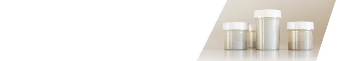
Solder Spheres
SnPb, In, BiSn and Lead-Free Solder Spheres
- Home

- Products
- Soldering Materials
- Solder Spheres
Solder Spheres
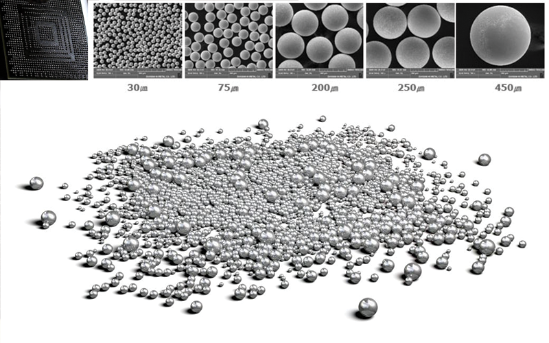
Solder spheres, commonly know as solder balls are the most common way to electrically interconnect flip chip semiconductors. CSPs , BGAS, LBGA are all arrays with small size factor that don't use bonding wires but use solder spheres beneath the package to aid with the miniaturization of the integrated circuits. Solder spheres come in multiple diamteres ranging from 0.075mm to 0.9mm and can fit in many package designs. There are multiple solder sphere alloys that can prove more or less reliable and can melt on a variety of temperatures. Normal spheres have a solidus (still solid) and a liquidus (liquid) temp with a gel like structure in between to aid with the bonding process. Eutectic solder spheres on the other hand have a very precise temperature where they switch from solid to liquid. This can help with tightly designed processes with very strict temperature requirements.
After many years of testing and debating, and with specific exceptions, the semiconductor industry has largely settled on the use of Tin (Sn), Silver(Ag), Copper(Cu) - or SAC - alloy for the assembly of lead-free products. Although the SAC alloy has been settled, which SAC alloy to use is still up for debate. North American and Europe manufacturers favor SAC305 (Sn3.0Ag0.5Cu), while Asian manufacturers generally favor SAC405 (Sn3.8Ag0.8Cu).
Whether you call them solder spheres or solder balls, CAPLINQ has been the premium supplier of solder balls since 2004. While many companies may offer solder spheres, very few companies offer the breadth and selection that CAPLINQ offers. Whether you are looking for eutectic Tin-Lead (SnPb) solder, high lead solder or lead-free variations, including Tin-Ag-Copper (SAC), Bismuth/Tin (BiSn), pure Tin (Sn), pure Indium (In) CAPLINQ has got you covered. We also offer low minimum order quantities and custom grades. Can't find the solder ball alloy you need? Let us know and we'll help you out.
 From
From
$54.55
LINQALLOY Bi57Sn42Ag1 | Near-Eutectic Pbfree Solder Spheres
- Leadfree Solder Spheres
- 1% Agg adds mechanical strength to bismuth-tin alloy
- Low-temperature near-eutetic Solder
- 4 weeks

SACQ | Pb-free Solder Spheres
- Leadfree Solder Spheres
- Excellent Solder Joint Reliability for small devices
- Excellent fatigue resistance
- 8 weeks
 From
From
$57.14 Bi58Sn42 | Eutectic Pbfree Solder Spheres
- Leadfree Solder Spheres
- Lowest Cost Eutectic (138°C) Solder
- Low-Temperature Eutectic Solder
- 4 weeks

CC-SAC305 | Copper Core SAC 305 Solder spheres
- SAC 305 alloy
- Core of the sphere is Copper
- Excellent fatigue resistance
- 8 weeks
 From
From
$333.33 In100 | Pure Indium Solder Spheres
- 100% Pure Indium Solder Spheres
- Soldering to non-metals
- Low Eutectic Melting temperature
- 4 weeks
 From
From
$25.00 SAC105 | Pb-free Solder Spheres
- Pb-free Solder Spheres
- Lowest cost Sn/Ag/Cu Alloy
- Excellent Fatigue Resistance
- In stock
 From
From
$26.80 SAC125N | PbFree Solder Spheres
- Lead-Free Solder Spheres
- Lowest cost Sn/Ag/Cu Alloy
- Nickel Dopped, hence the SACNi name
- In stock
 From
From
$29.50 SAC305 | Pb-free Solder Spheres
- Leadfree Solder Spheres
- Lowest cost Sn/Ag/Cu Alloy
- Excellent Fatigue Resistance
- In stock

SAC387 | Pb-free Solder Spheres
- Pb-free Solder Spheres
- For BGA and CSP components
- Tin/Silver/Copper alloys
- 4 weeks
 From
From
$24.35 SAC396 | Pb-free Solder Spheres
- Pb-free Solder Spheres
- Excellent Solder Joint Reliability
- Best Wetting Sn/Ag/Cu Alloy
- 4 weeks
 From
From
$29.50 SAC405 | Pb-free Solder Spheres
- Pb-free Solder Spheres
- Excellent Solder Joint Reliability
- Best Wetting Sn/Ag/Cu Alloy
- In stock
 Solder Spheres")
Sn100 | Pure Tin (4N) Solder Spheres
- Pure Tin
- Most important application electroplating
- Proven choice for coating of package leads and terminals
- No longer available

Sn10Pb90 | High melting point Solder Spheres
- Medium Solidus/Liquidus transition
- High Liquidus temperature (301°C)
- Ideal for automotive applications
- 4 weeks
 From
From
$57.14 Sn5Pb95 | High melting point Solder Spheres
- Low Solidus/Liquidus transition
- High Liquidus point (322°C)
- Ideal for automotive applications
- 4 weeks
 From
From
$43.75 Sn63Pb37 | Eutectic Solder Spheres
- Eutectic Solder Spheres
- Tin lead
- For BGA and CSP components
- 4 weeks
 From
From
$89.44 Sn96.5Ag3.5 | Eutectic Pbfree Solder Spheres
- Leadfree Solder Spheres
- Eutectic Melting Temp of 221°C (430°F)
- The highest Joint Reliability
- 4 weeks
Product Selector Guide
| Alloy Type | Tin-Lead/ Pb-free | % Metal Loading | Melting Temperature | Remarks | ||||||||||
|---|---|---|---|---|---|---|---|---|---|---|---|---|---|---|
| Tin (Sn) % | Lead (Pb) % | Bismuth (Bi) % | Silver (Ag) % | Copper (Cu) % | Indium (In) % | Eutectic (°C) | Solidus (°C) | Liquidus (°C) | ||||||
| Sn63Pb37 | Tin-Lead | 63 | 37 | - | - | - | - | 183 | - | - | Eutectic Tin-Lead | |||
| SAC105 | Pb-free | 98.5 | - | - | 1.0 | 0.5 | - | - | 220 | 225 | Lowest Silver Content | |||
| SAC125N | Pb-free | 98.3 | - | - | 1.2 | 0.5 | - | - | 217 | 219 | 0.05% Nickel (Also called SAC125Ni) | |||
| SAC305 | Pb-free | 96.5 | - | - | 3.0 | 0.5 | - | - | 217 | 221 | Industry Standard Pb-free | |||
| SAC387 | Pb-free | 95.5 | - | - | 3.8 | 0.7 | - | - | 217 | 219 | Special Application Pb-free | |||
| SAC396 | Pb-free | 95.5 | - | - | 3.9 | 0.6 | - | - | 217 | 221 | Industry Standard Pb-free | |||
| SAC405 | Pb-free | 95.5 | - | - | 4.0 | 0.5 | - | - | 217 | 225 | Highest Silver Content | |||
| SACQ | Pb-free | 92.45 | - | 3 | 4 | 0.5 | - | - | 216 | 211 | ||||
| Sn96.5Ag3.5 | Pb-free | 96.5 | - | - | 3.5 | - | - | 221 | - | - | Eutectic Leadfree High Silver | |||
| Sn100 | Pb-free | 99.9928% min | - | - | - | - | - | 232 | - | - | 4N Pure Tin (>99.9928% Sn) | |||
| Bi58Sn42 | Pb-free | 42 | - | 58 | - | - | - | 138 | - | - | Eutectic Low-Temp Bismuth-Tin | |||
| Bi57Sn42Ag1 | Pb-free | 42 | - | 57 | 1.0 | - | - | - | 139 | 140 | Near-Eutectic Low-Temp Bismuth-Tin | |||
| Sn5Pb95 | Tin-Lead | 5 | 95 | - | - | - | - | - | 312 | 322 | High melting point Solder Spheres | |||
| In100 | Pb-free | - | - | - | - | - | 100 | 156.6 | - | - | Pure Indium Solder Spheres In100 | |||
Low volume flexibility, high volume pricing
CAPLINQ maintains an inventory of many sphere alloys and sizes, and we specialize in the fulfillment of small orders. CAPLINQ also offers volume breaks and discounts for our higher volume customers. A complete list of sphere diameters, packaging quantities, volume breaks and discounts can be seen by clicking on the product Alloy Type below
Frequently Asked Questions
Frequently Asked Questions about Solder Spheres
What\'s the difference between solder spheres and solder balls?
There is no difference between solder balls or solder spheres. Because solder balls do not sound very high tech and balls do not technically have a tolerance, the industry moved to the naming convention of solder spheres. Solder spheres are now more common and solder sphere diameter and spheroid tolerances can now be measured and defined.
Why are the jumps in price breaks so high?
Solder spheres ultimately end up being made-to-order products with a limited shelf-life once produced. Furthermore, there is a lot of "start-up material" that is wasted at the beginning of each production, whether it is for 1 jar or 1000 jars. These wastes are calculated into the lower volume pricing and is the reason the price jumps are as high as they are.
What is the tolerance of your solder spheres?
The tolerance of the solder sphere depends on the size of the sphere. It can generally be summarized as 1.5% of the solder diameter. A more complete answer on the solder sphere tolerance can be found here.
What size solder sphere defines whether it is for BGA, CSP or FlipChip?
There are no hard and fast rules for this, though generally, as solder spheres get smaller, they are used from BGAs to CSPs to Flipchip devices. Typically, it can be said that BGA solder balls are greater than 0.250mm in diameter and bigger, CSP are between 0.100mm and 0.250mm in diameter and flip chips use solder balls that are 0.100mm and under in diameter.
What is the shelf-life of solder spheres in tape and reel packaging?
The guaranteed shelf-life of solder spheres in tape and reel packaging is 1 year from the date of manufacture. There are simply too many variables to be able to account for all the possible scenarios of long term storage of the solder spheres in the tape and reel. In the jars, the solder spheres are preserved in an inert gas (nitrogen). In the tape & reel, the spheres are no longer in the inert gas, but are vacuum sealed, removing air from the individual package
The reason for the shelf-life is to limit the liability during the period in which we have a 100% confidence that the solder spheres have not oxidized. This confidence decreases as the time increases and the storage conditions are unknown.
To the best of our knowledge, the risk of oxidation when the reels are kept in cool, dry conditions are minimum, even for several months (or maybe even years) after the published shelf-life. We cannot officially increase the shelf-life without having scientific data to support this, but we do not believe there is any negative consequence to using the solder spheres beyond the published shelf-life date.
What is the work life of Solder Spheres?
For the solder sphere we don't spell out the work life in the Datasheet, because the alloys used in solder spheres are formulated to resist oxidation at room temperature. This means they won't significantly degrade just by being exposed to air after opening the container. Common practice is to mention the shelf life and storage conditions to maintain the optimal performance of the solder spheres. The product should be stored in sealed containers and should not be refrigerated. Probing of spheres in jars with fingers or other implements can damage the material by changing its shape or scoring the sphere surface or by contaminating the material. This could result in sphere placement difficulties.
Can I store solder spheres back to the jar?
Generally, we don't recommend putting unused spheres back into the original jar to avoid any potential contamination. Even with careful handling, there's a risk of introducing contaminants like skin oils, dust, or moisture into the jar when putting spheres back. This can affect the solderability of the spheres. We typically recommend using a complete jar at a time. Solder spheres are packaged in a nitrogen atmosphere to minimize oxidation. Opening and closing the jar can displace some of the nitrogen, potentially increasing the oxidation rate of the remaining spheres. You could use a separate moisture proof container to store your unused spheres.
Learn More
The evolution from lead-containing Sn63Pb37 wire to Pb-free micron-sized solder spheres
Semiconductors and printed circuit board technology are relentlessly evolving industries. Their constant development has forced solder technolgy to change and evolve too. Solder technology, as a whole, has moved from lead-based solder wire and separately applied solder flux to solder spheres. The latest industry break-through being a move away from wire bonding to micron size solder spheres for flipchips. To understand how this happened let\'s start by breaking down the product name Sn63Pb37 into its parts:
- Sn = Tin
- 63 = 63%
- Pb = Lead
- 37 = 37%
Alloys melt at different temperatures based on their composition or ratio of metals. Sn63Pb37 solder liquifies at exactly 183°C. Because the liquidus phase is so perfectly defined, Sn63Pb37 is known as a eutectic solder. This is very useful for two reasons. The first is that there is no "slurry phase" as some of the metals melt and others have not yet melted. The second is that the 183°C temperature is incredibly useful for circuit boards because it was high enough to melt the solder but low enough not to damage plastic components or the circuit board itself.
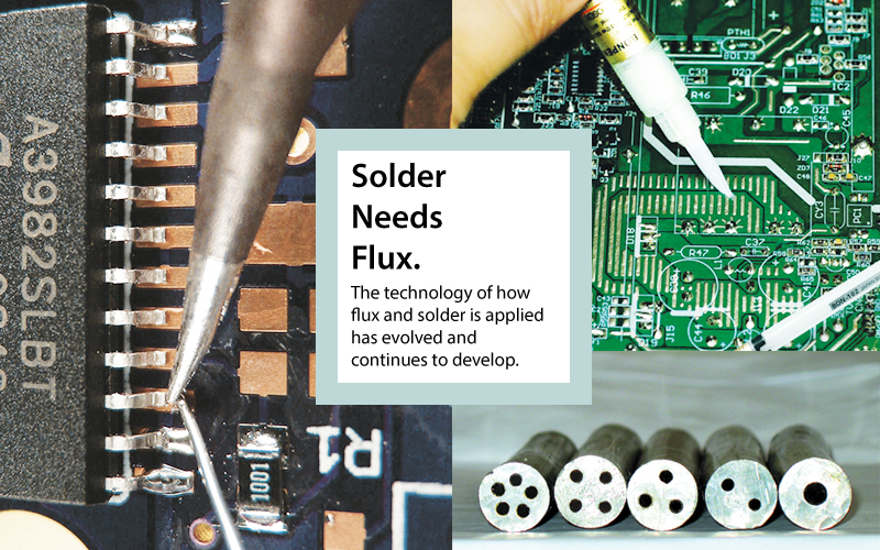
Solder wire needs flux. Flux removes oxidation.
Without flux the layer of oxidation acts as a barrier between the solder and the two conductive contact points thus preventing a clean and solid solder joint.
Pre-coating parts in flux was, therefore, an essential extra step that cost more time and labor. So the next step in solder development was hollow solder wire filled with an internal flux. Further developments included multi-core wire with multiple hollows for better distribution of flux.
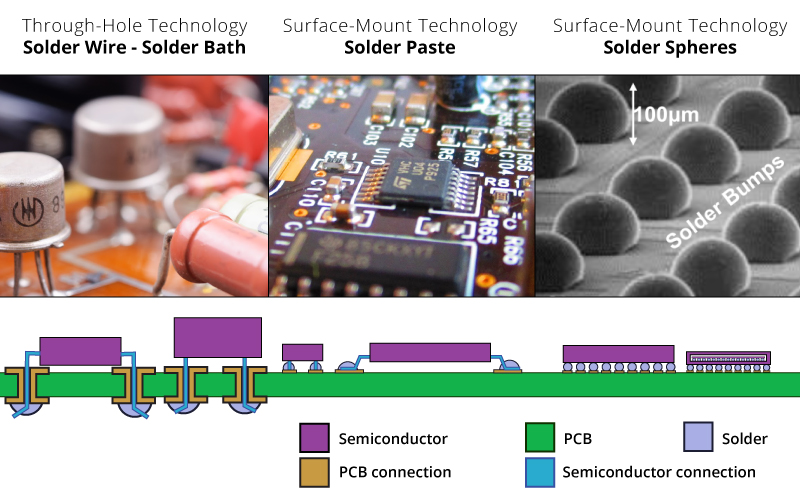
The industrial mass-produced Printed Circuit Board (PCB), as we know it, started out with through-hole technology. Semiconductor devices and chips had pins which were pushed through holes in the printed circuit board. The bottom side of the entire circuit board would then have flux applied in one go and then be dipped into a solder bath. This automated the soldering process and eliminated unnecessary extra steps. Which, in terms of mass production, saved millions of dollars in energy and material.
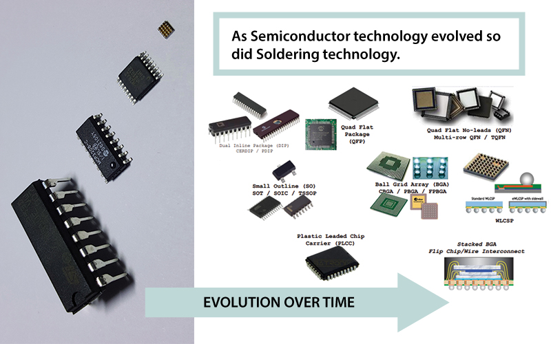
Evolving ICs – Pushing soldering technology to evolve
After through-hole technology PCBs evolved towards surface mounted technology: where solder paste was used. Solder paste is a suspension of powdered flux and powdered solder together. This allowed solder to be printed on circuit boards by a solder paste printer and then melted in one go in a solder reflow process: thereby allowing for much more complex and densely packed installations of semiconductors on the PCB.
Integrated circuits have been getting smaller and smaller and with larger and larger numbers of tiny transistors. This can be best seen in the evolution of Small Outline Integrated Circuits or SOIC: evolving at first by doubling the number of inputs and outputs or pinouts: from SO8, on to SO16, SO32. Eventually for the sake efficiency, instead of two rows of pinouts, all four sides would be used in the Quad Flat Pack (QFP). This also meant that the legs got thinner and thinner and got packed closer and closer together.
Array packaging moved semiconductor packages from wire bonding to solder balls
When you are using all four sides and even stacking wafers what can you do to further increase the number of inputs and outputs? The answer turned out to be: use the bottom of the chip as well. So, instead of many small thin legs, solder spheres would be placed directly on the bottom of the chip and would act as the connection between the Ball Grid Array (BGA) and the circuit board. This meant full encapsulation in an epoxy molding compound was no longer necessary and you could simply use an underfill.
250,000 solder spheres: sounds like a lot, but at micron sizes, that’s just enough for a heaped tablespoon full. Eventually, solder spheres got smaller and smaller so that they could pack even tighter grids of connection on the bottom of silica die. In these flip chips setups, tiny solder spheres are used instead of even 25-micron thick gold wire. Solder spheres are made in an amazing process with incredible accuracy and tight quality control.
A parallel evolution in material: from Lead (Pb) to Lead-free!
Early in the 2000’s in Japan, Sony and other concerned companies started to push for lead-free solder. This was in response to a situation in which electronic devices were ending up in landfills, and these landfills were in turn exposed to rainwater which allowed the lead in the solder to contaminate the groundwater. In 2006 the EU Restriction of Hazard Substances Directive (RoHS) came into effect restricting the use of lead consumer electronics.
This led to SAC305 Lead-free solder replacing eutectic SnPb63/37 solder as the industrial standard: with 75% of companies using it. Here is what the name means:
- S = Tin
- A = Silver
- C = Copper
- 3 = 3% Silver
- 05 = 0.5% Copper
As a near eutectic solder it has adequate thermal fatigue properties, strength, and wettability. Another advantage of SAC solder is that it’s more resistant to gold-embrittlement and has substantially higher joint strength than PB solders.
Going Pb-free however means using silver instead of lead which means increases costs. For some applications SAC solders with less silver are suitable. These include SAC105, Bi57Sn42Ag1, as well as silver-free and lead-free solder , Bi58Sn42.
Using silver means that SAC solders have a 34°C higher melting point than Sn63Pb37 solder at between 217-220°C. This requires a higher solder reflow temperature of 235-245°C in order to achieve wetting and wicking. Some printed circuit components are susceptible to SAC assembly temperatures: including capacitors, optoelectronics etc.
Companies have since started offering 260°C compatible components to meet the high temperature required for SAC solder reflow. 260°C compatibility is fast becoming the new standard for semiconductor and component manufacturers.
High Tech Tin
CAPLINQ is not only able to supply the alloys and purify the solder material, but it has an innovative diameter and spheroid selecting system of solder balls and an advanced anti-oxidation technology that actually dopes an anti-oxidation element into the alloy in addition to its OSP surface coating process.
Not only are our solder spheres High-Tech, but they are made from a unique uniform droplet spraying technology that far outperforms competitors in terms of productivity. This combination of high technology and high productivity allow CAPLINQ to offer its customers the best value for the best product.
| Solder ball diameter (mm) | Variation | Pitch size |
| 0.75 | 0.90 - 0.65 | 1.50, 1.27 |
| 0.60 | 0.70 -0.50 | 1.0 |
| 0.50 | 0.55 - 0.40 | 1.00, 0.80 |
| 0.45 | 0.50 - 0.40 | 1.00, 0.80, 0.75 |
| 0.40 | 0.45 - 0.35 | 0.80, 0.75, 0.65 |
| 0.30 | 0.35 - 0.25 | 0.80, 0.75, 0.65, 0.50 |
| 0.25 | 0.28 - 0.22 | 0.40 |
| 0.20 | 0.22 - 0.18 | 0.30 |
| 0.15 | 0.17 - 0.13 | 0.25 |